(Click on pictures to enlarge)
Also see my personal (non-ham) home page at
www.cbjohn.com
Psalms 111:2
I have been designing and producing microprocessor-based digital tuners (VFOs) for amateur radios since about 1997, some of them
shown below. After documenting and publishing articles about the tuners in QST or QEX and starting to sell them as kits through my friends
at various marketing channels, I'm finally taking the time to design and build complete radios of my own. Hams around the world were
using my kits immediately, building them into radios and making contacts with them, but I was always working on customer support or the next,
more advanced versions of the products and didn't take the time to build a complete radio myself.
The two project below (first the MiniDC 40M Transceiver and then the Phasing Rig) were started when I finally
got around to building complete radios for myself, experimenting with various circuits, techniques and parts that I had read about. Not
intending to make these radios into kits to sell gave me great freedom to use any kind of parts or techniques that I wanted.
Experimenting with MANY variations of circuits and making measurements as to how well they work has been exciting and personally rewarding.
Sharing the designs with friends around the world who are with me on this journey is also an important part of why I am doing this.
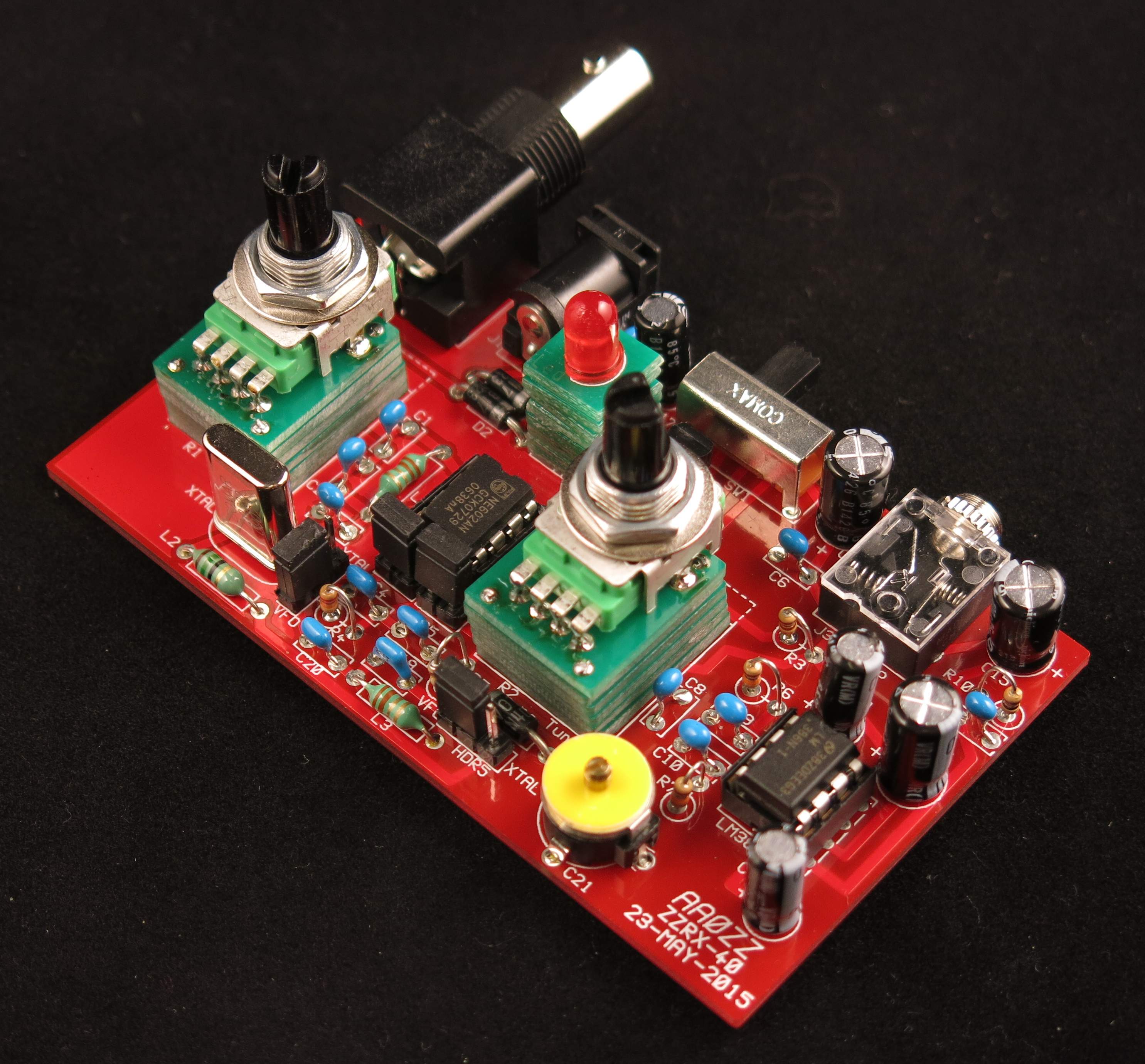
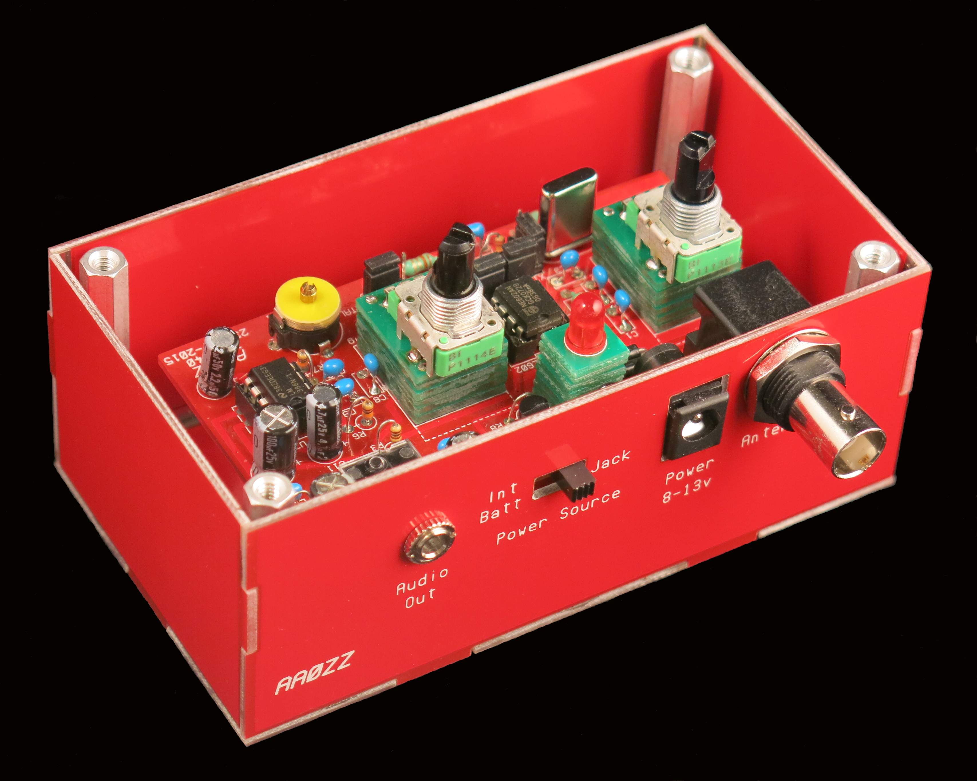
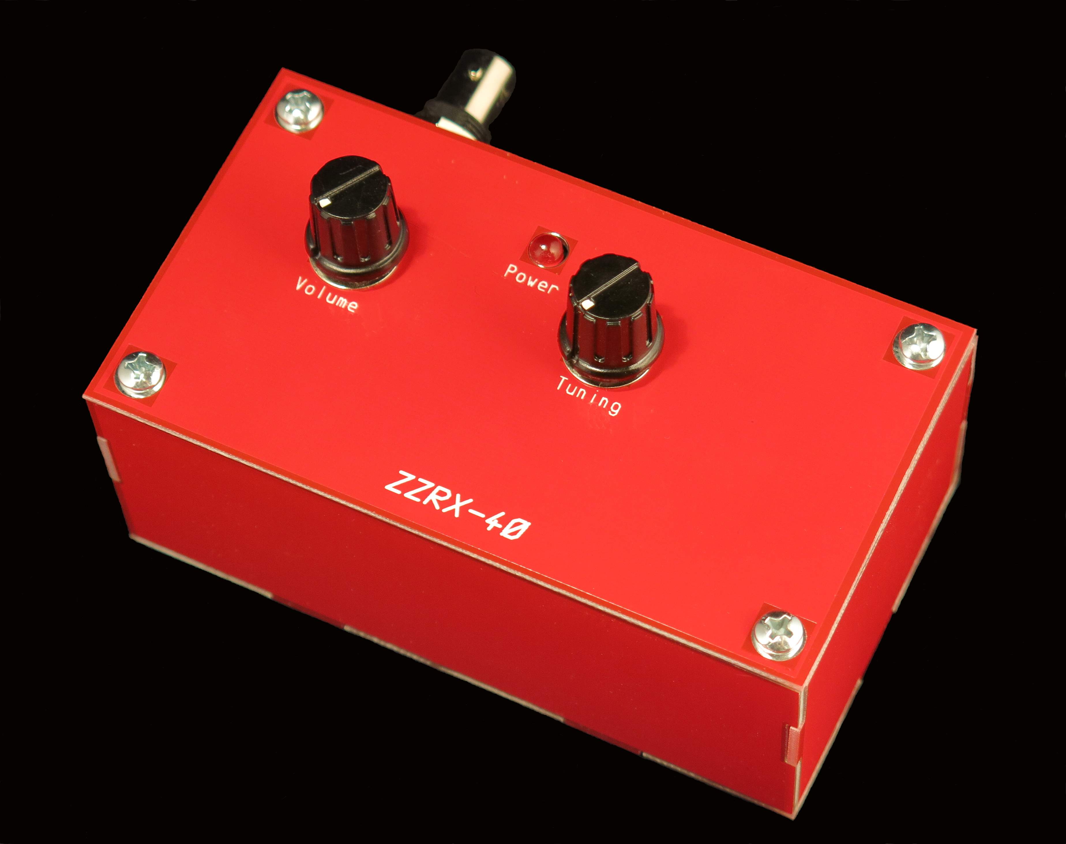
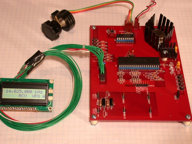
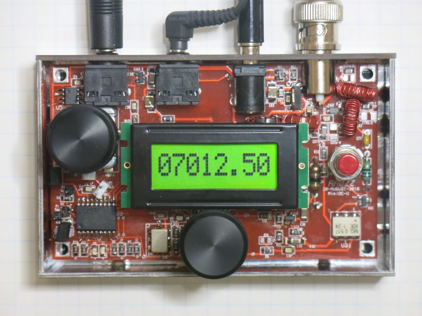
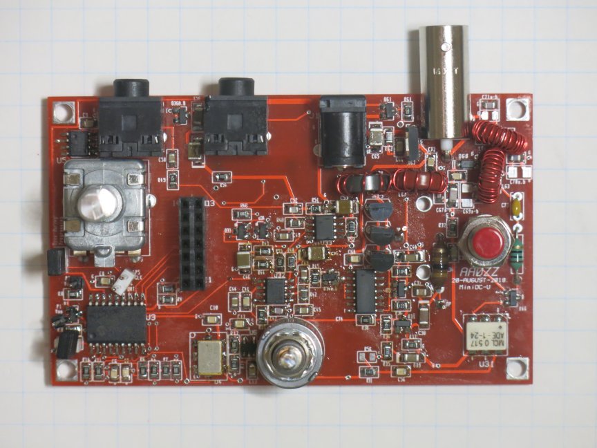
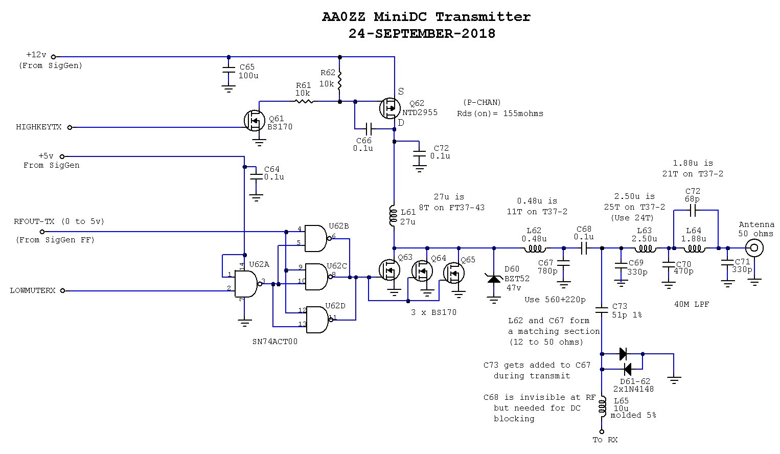
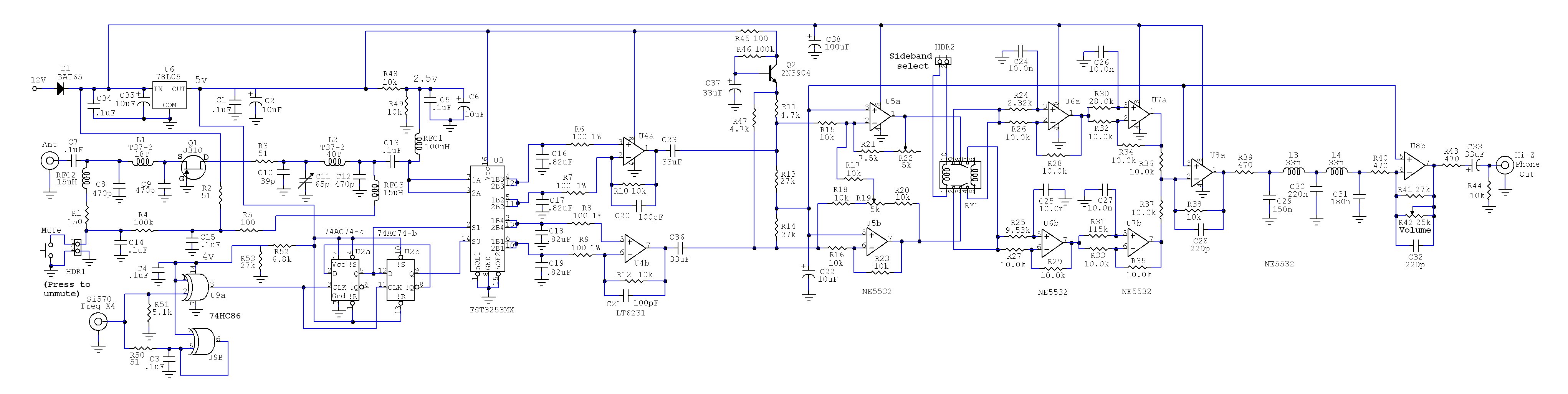
40M Direct Conversion CW Transceiver Dimensions: 4" x 2.5" x 0.75"
This project originated as challenge from my good friend Dave Benson, K1SWL, in October, 2017. It was
Dave wondered if we could make a complete 40M transceiver that would fit into this box. We decided it should
It should have a built-in CW keyer to construct the DIT and DAH elements.
We wanted the transmitter that put out about 5 watts.
Dave is a very experienced designer he quickly developed his using an Arduino and a Si5351 RF generator.
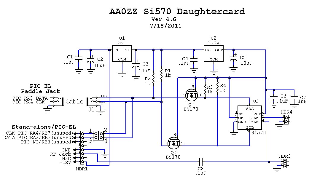
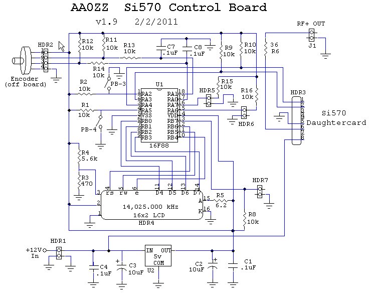
I built mine with a small PIC microcontroller (16F88) controlling a Si570 Programmable PLL for the RF local
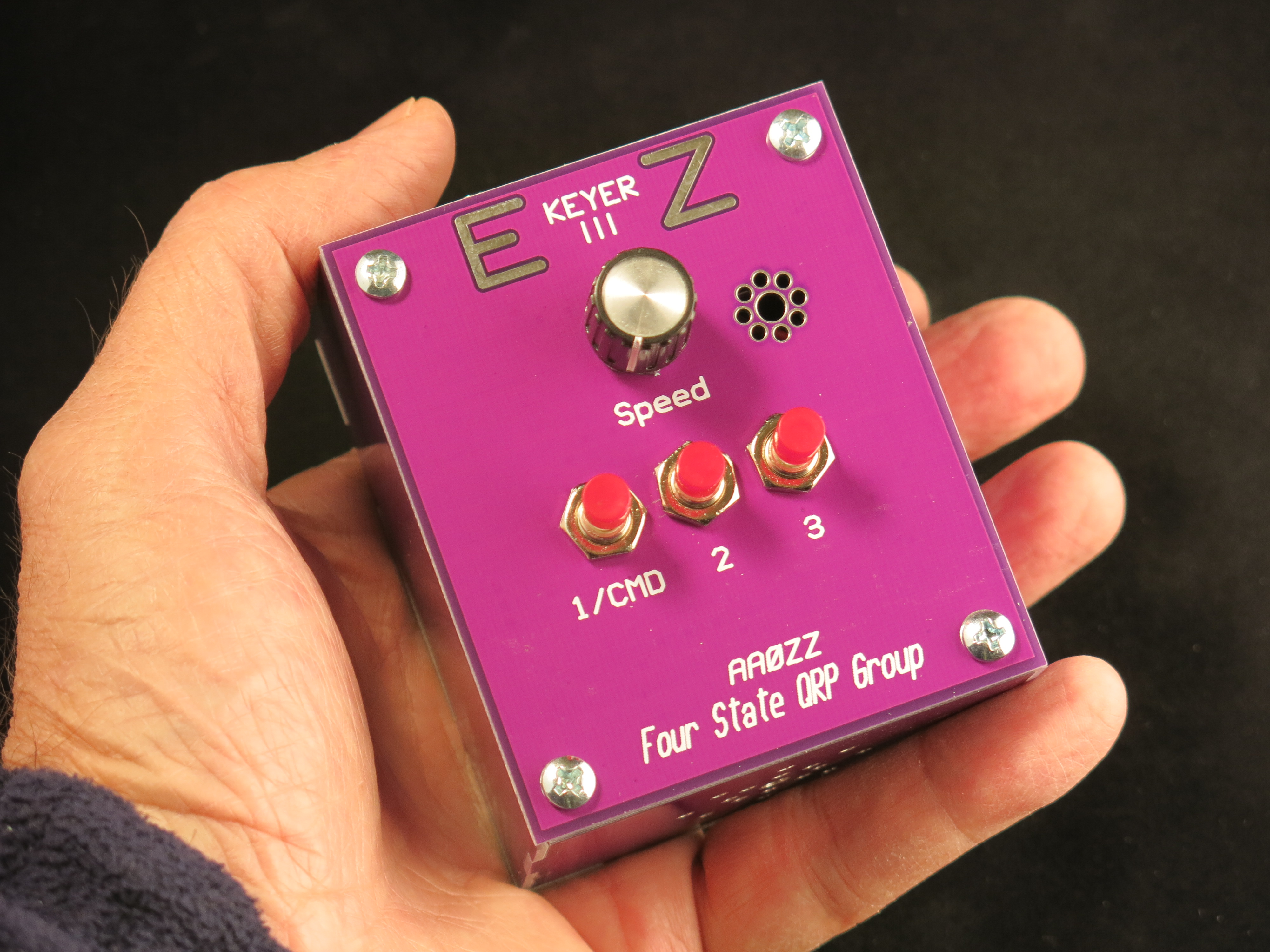
I used another small PIC microcontroller (16F1822) for a stripped-down version of my stand-alone EZKeyer
I programmed both PICs with assembler code.
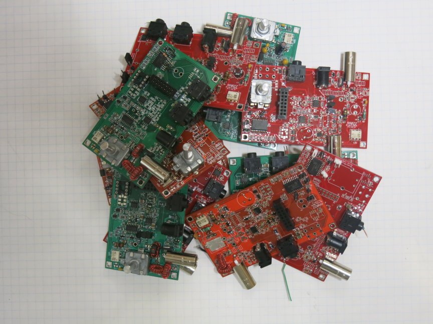
After about 25 PCB iterations (!!) and lots of experimentation, this is what I came up with. Most of the
MiniDC with no case, LCD, knobs (JPG)
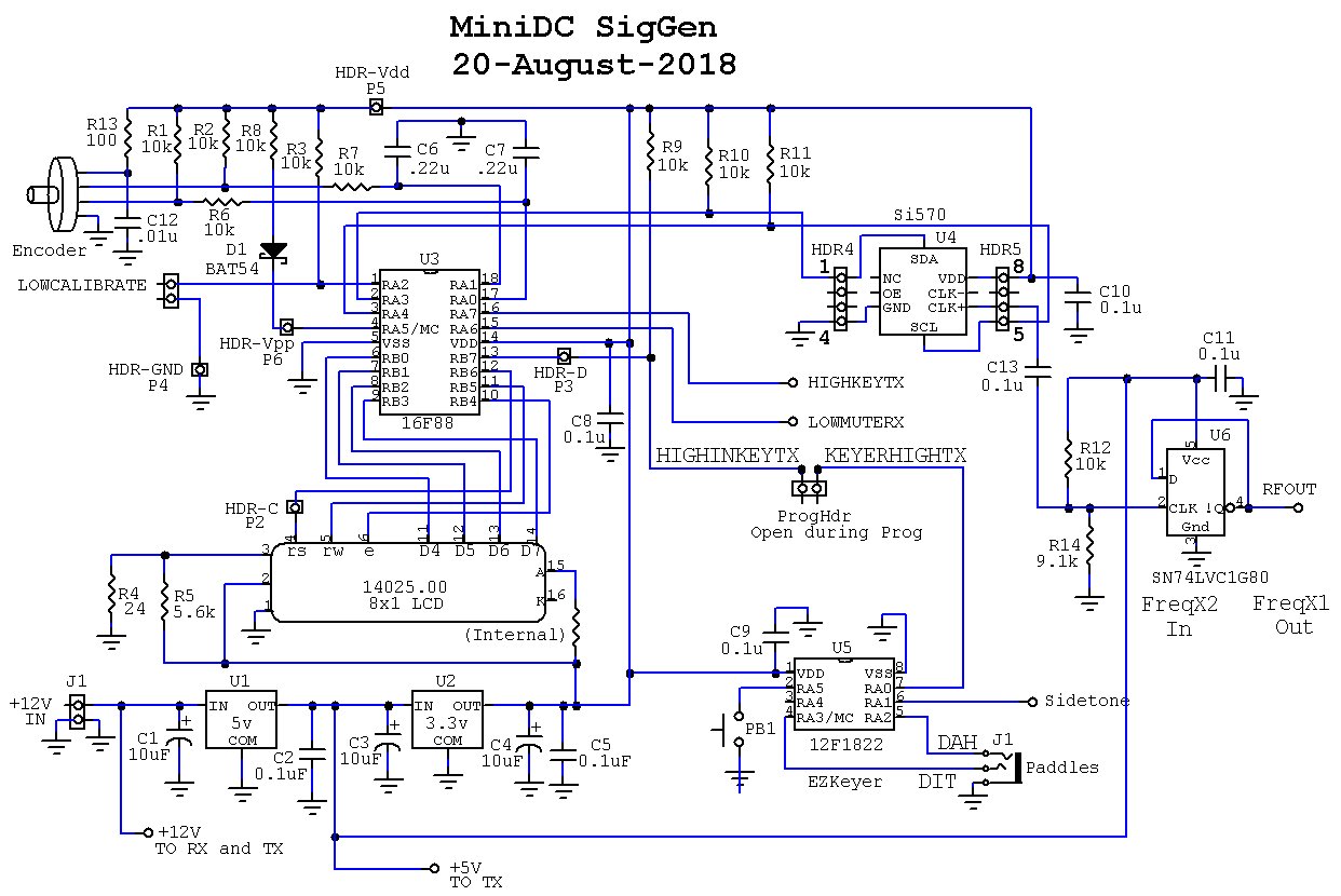
Signal Generator Schematic (JPG)
"Boneyard" of forgotten MiniDC favorites (JPG)
This transceiver works well. I have used it to "talk" (using Morse code) to many hams all around the country. Since
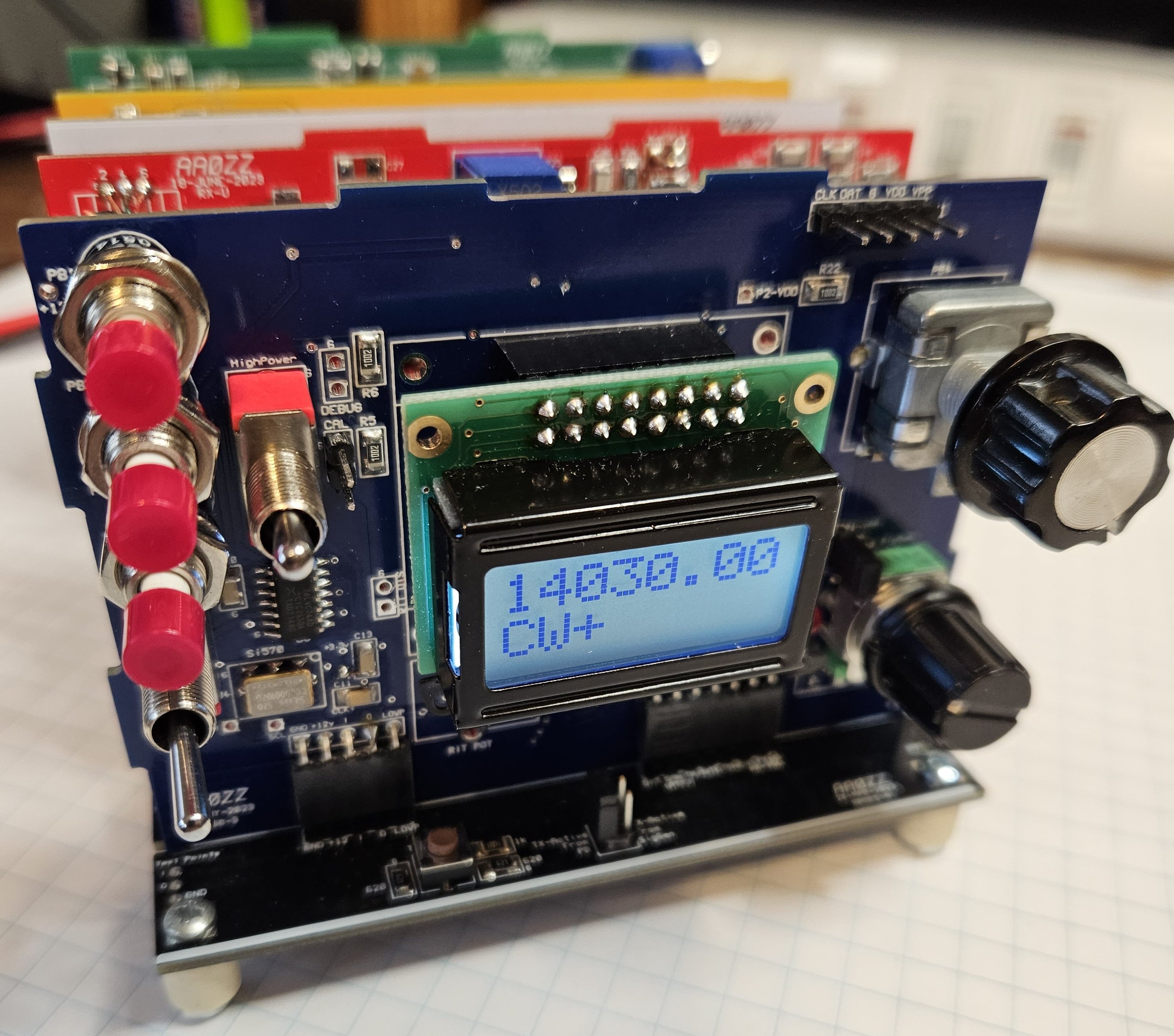
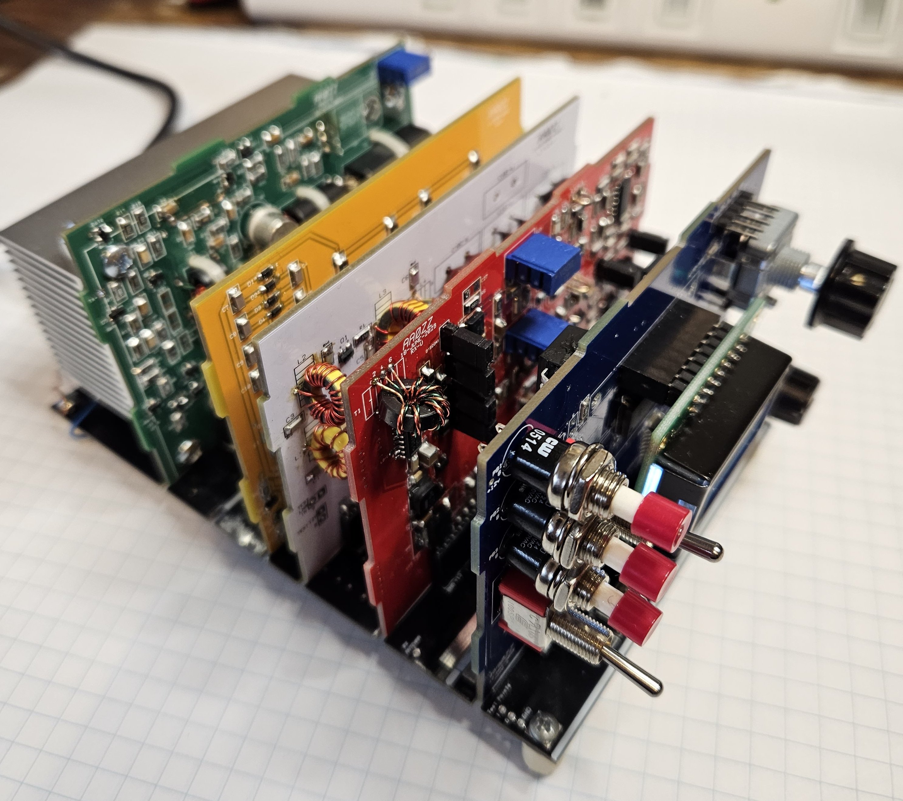
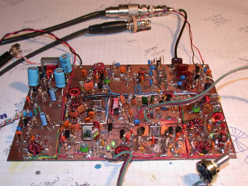
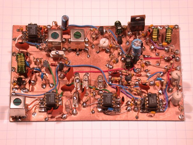
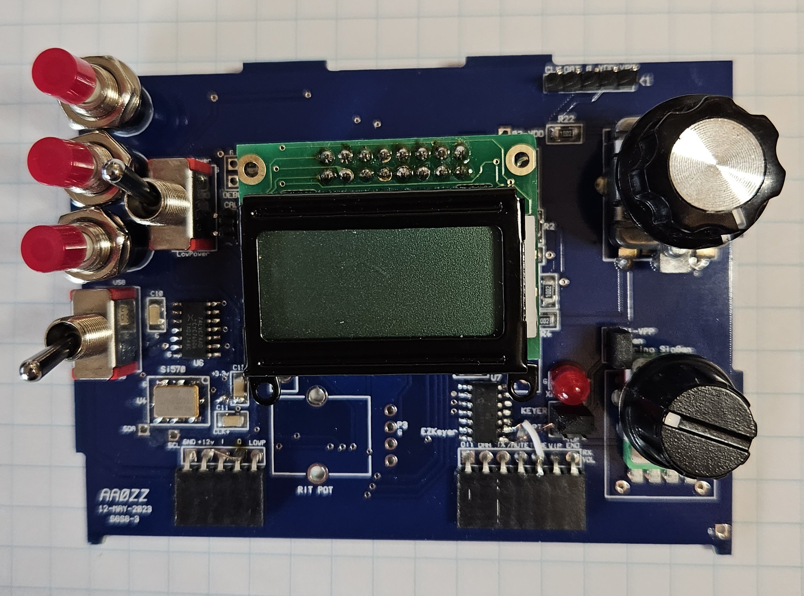
This is the second "frozen" version of my Phasing Rig with 5 plug-in boards on a base board. It will eventually have side, top,
and front panels. This version and is usable on 40M, 30M, and 20M.
My next step will be to add Single Sideband (voice) capabilities. I "may" dig out a microphone and make some phone contacts
but my main reason is to get the radio on the digital modes - PSK31 in particular, since this mode lends itself to conversational QSOs instead of just quick computer interchanges.
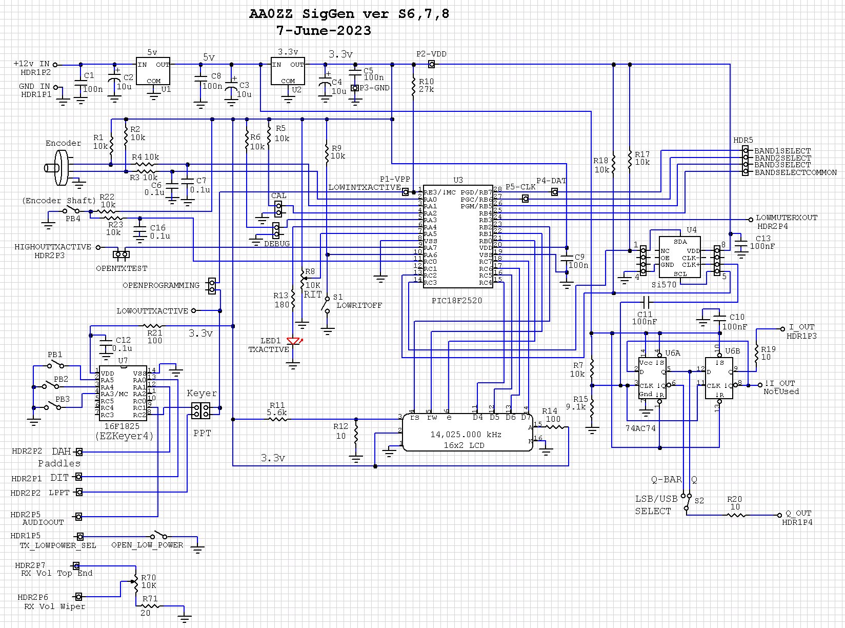
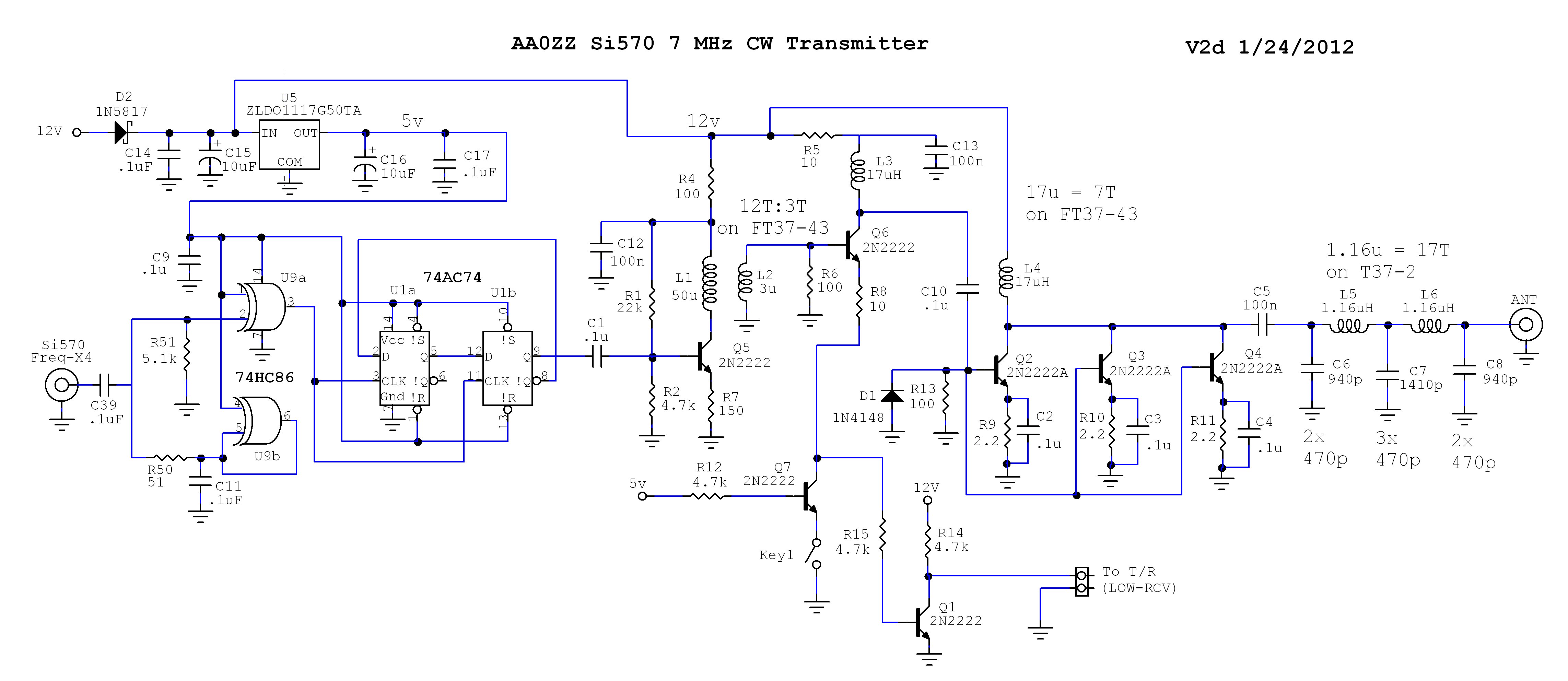
Here's a rundown of the various plug-in boards. 1a) Signal Generator Board (JPG)
1b) Signal Generator Schematic (JPG) The Signal Generator has 2 PIC microprocessors. The 28-pin 18F2520 controls the Si570 RF source, the 2x8 character LCD,
the rotary encoder, the various switches, and the Transmit/Receive switchover driver.
The main PIC communicates with a small 8-pin PIC (12F1822) which has a stripped-down version of my EZKeyer to generate the DIT and DAH elements for keying the CW transmitter.
This version has three pushbutton to control the keyer's menu, change speed, and to send one of the three canned messages. The main PIC also switches
the rig's operation between transmit and receive mode.
A note about QSK. QSK means the ability of the rig to switch fast enough between transmit and receive mode to be able to hear the other
station's DITs and DAHs between the transmitted DITs and DAHs. Switchover time for this rig about 8 ms which is exceptional! The other station can be heard even when
transmitting at 55 words per minute, the fastest speed my EZKeyer can go. Try that with your commercial rig! My Elecraft K2, in "full QSK mode", can only hear the other
station when transmitting at 19 WPM at less. My Elecraft KX2 is about the same - 19 WPM or less and the same for my Kenwood TS-940. Most QRP rigs, such as the Elecraft K1,
are only good for QSK when transmitting up to about 8 WPM. (For many folks this is just fine. They don't care if they are unable to hear between the elements when sending CW.)
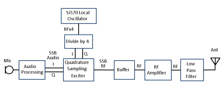
This version has a toggle switch to switch between upper sideband and lower sideband. This is done by reversing one of the
quadrature output signals (the Q-bar signal). This changes the quadrature relationship between the I and Q. After this, the remainder of the circuitry in the receiver is common
for both modes so minimal adjustments (if any) are needed.
No component differences are introduced.
The RIT mechanism is there but not debugged in software yet.
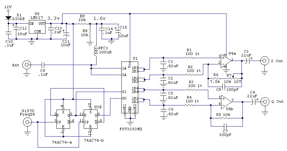
The Signal Generator will be the "front" board so it also has the volume control for the receiver. The Signal Generator board has had 15 about PCB revisions. 2b) Phasing Receiver Board (JPG)
2b) Phasing Receiver Schematic (Left Side) (JPG)
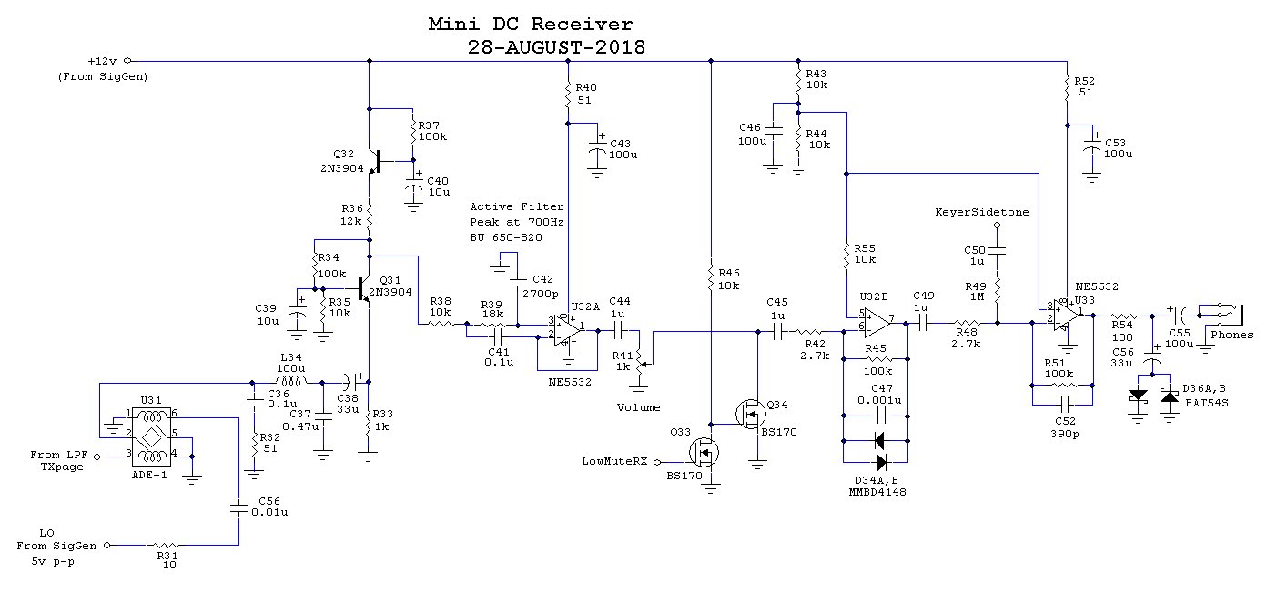
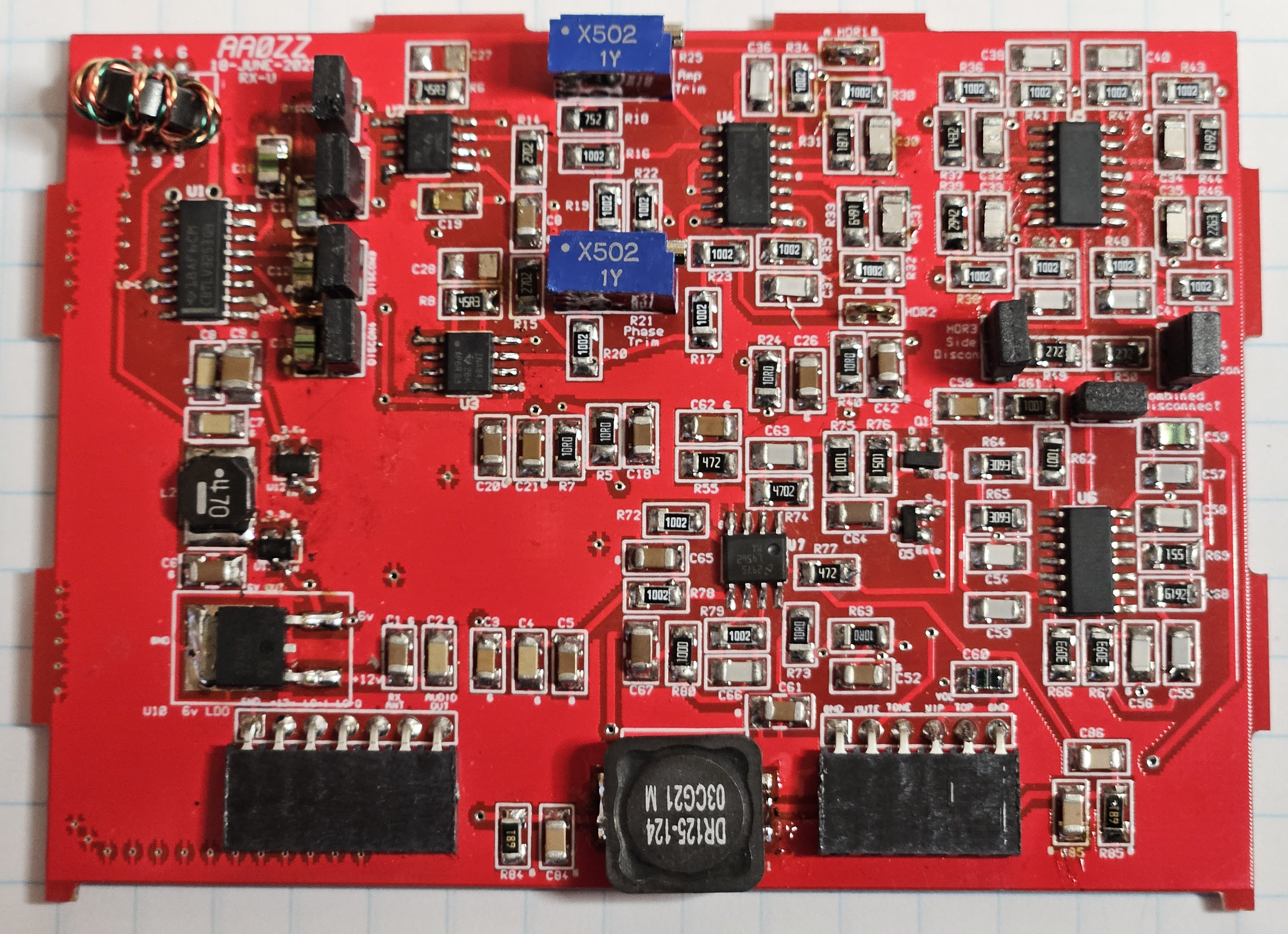
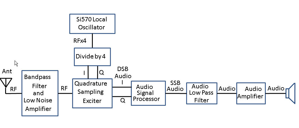
2c) Phasing Receiver Schematic (Right Side) (JPG) The receiver uses a Quadrature Sampling Detector (QSD) front-end, an audio phasing section (for single-sided reception) which is a take-off from
Rick Campbell's (KK7B) R2Pro, an audio bandpass filter, and an audio amplifier.
One important change in this version is the capacitive coupling between the front-end multiplexer and the two instrumentation amplifiers (INAs). This was necessary
to eliminate the imbalance between the outputs of the two INAs. Since the INAs provide huge amplification, any slight imbalances in the inputs
produce large imbalances in the outputs that are difficult to compensate for in the balancing circuitry to follow. The capacitive coupling
(capacitors C14 - C17) require additional circuitry to re-bias the inputs at the reference level. This results in two nicely balanced outputs.
High quality (low noise) INAs are essential for this usage since the noise factor of the receiver is largely determined here.
Opposite sideband suppression is terrific - about 54 dB (measured). The Minimum Discernable Signal (MDS) is good at about -125 dBm.
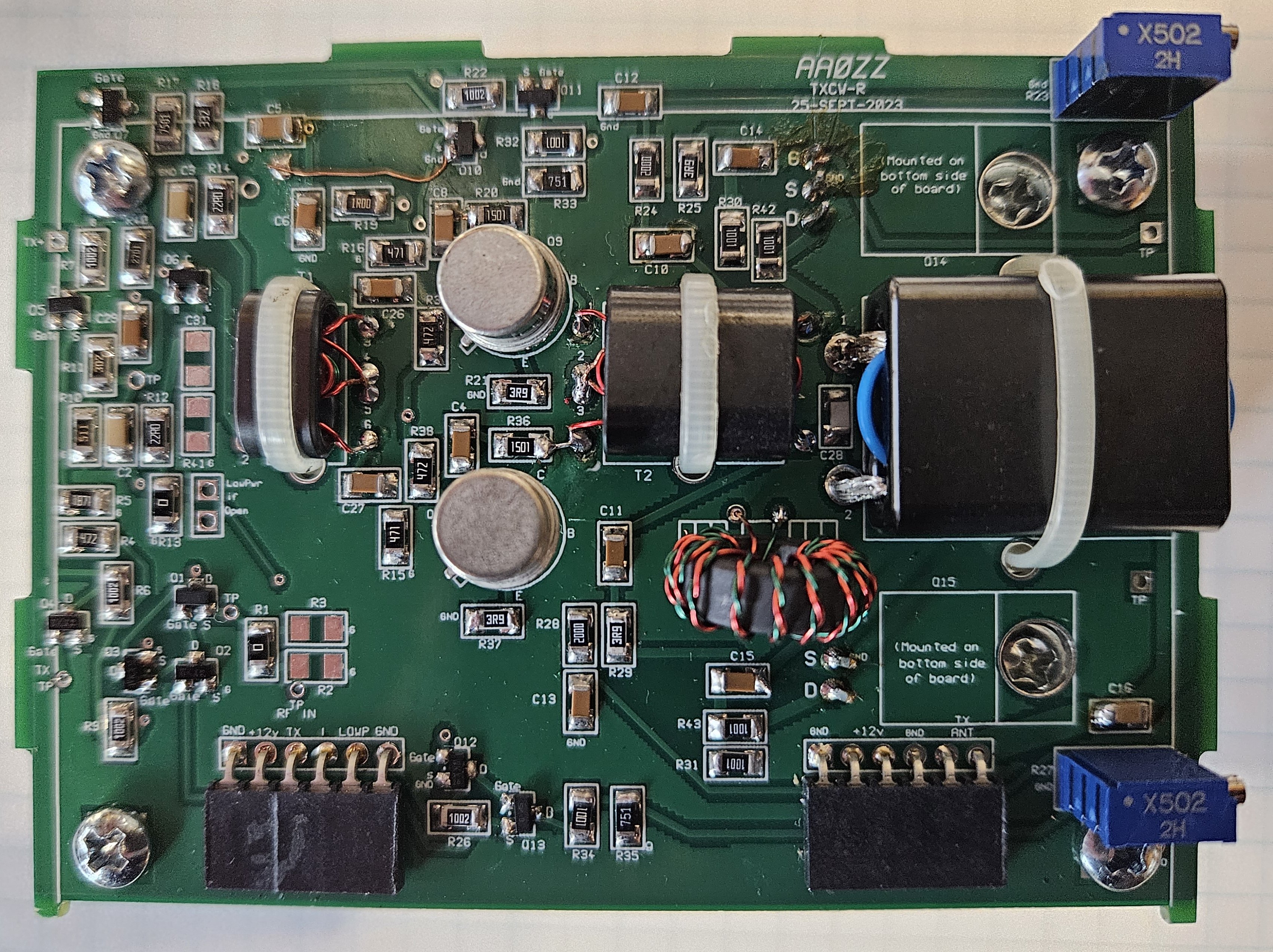
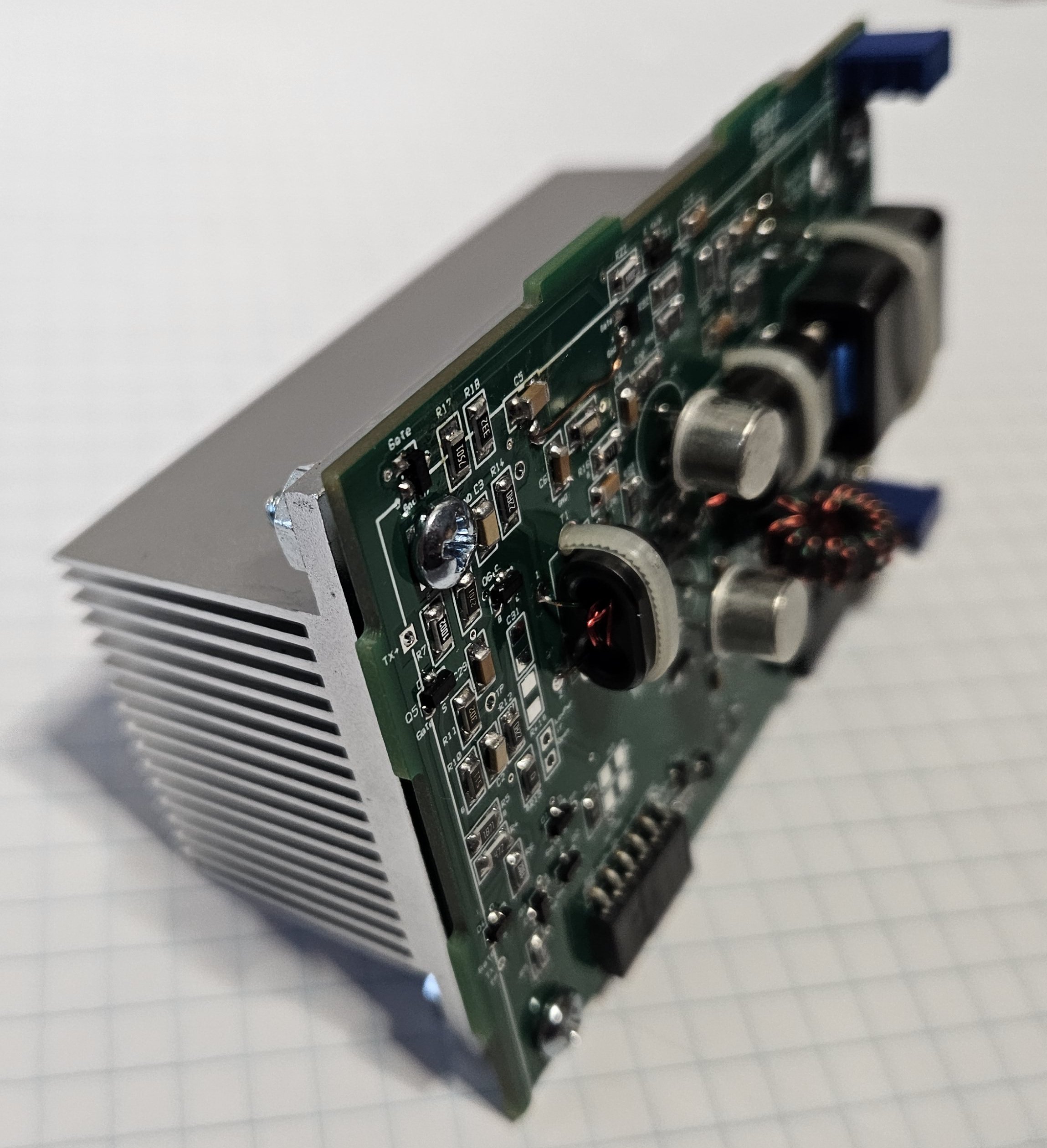
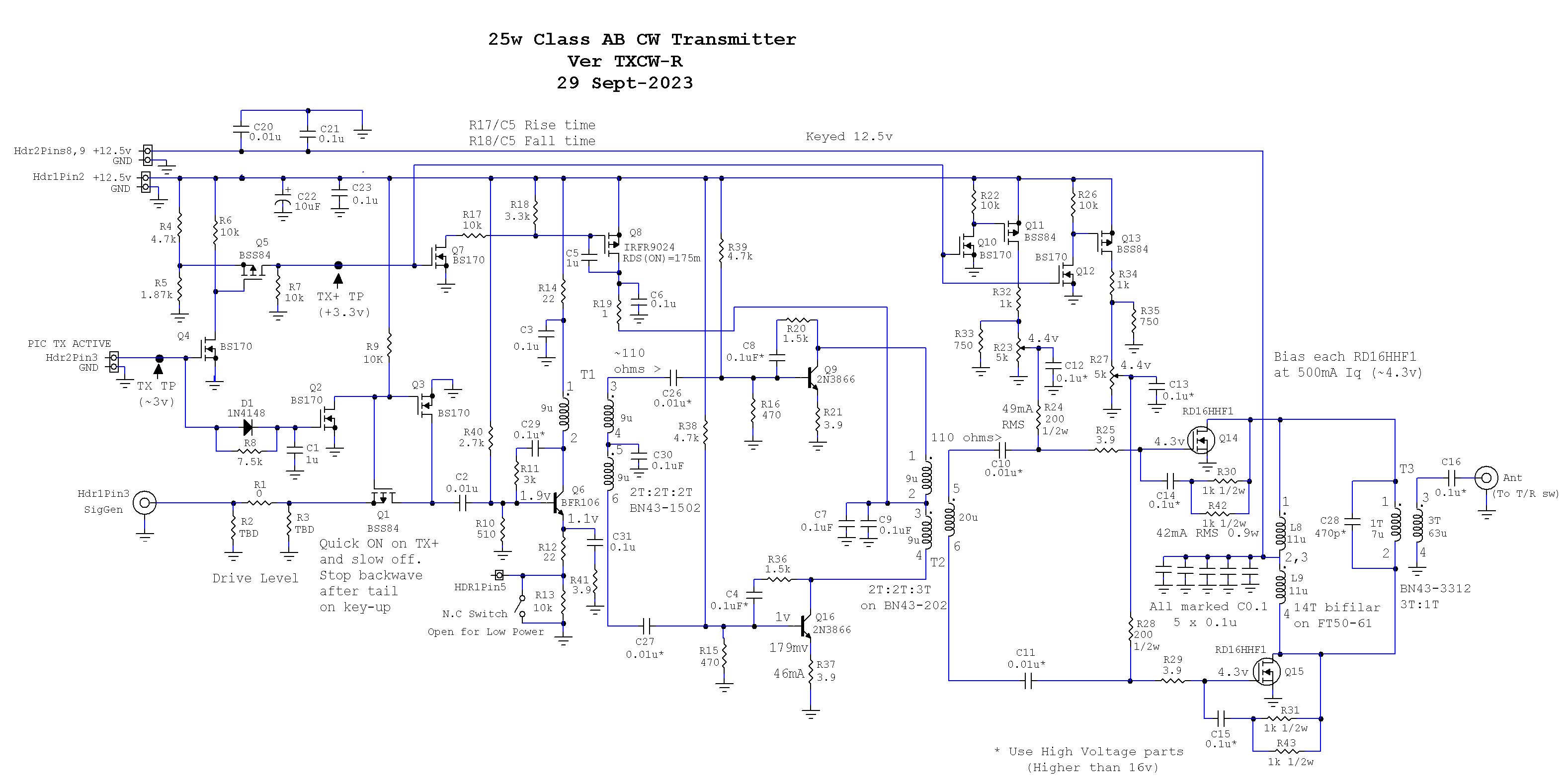
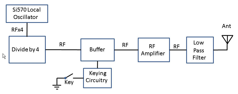
The receiver board has gone through at least 50 PCB revisions! I'm glad they are so inexpensive! 3a) 30W CW Transmitter Board (JPG) 3b) 30W CW Transmitter with heat sink (JPG) 3c) 30W CW Transmitter Schematic (JPG) This version of the transmitter is CW only but it runs in Class AB so it will be used later as the amplifier for a separate SSB/digital exciter plug-in board.
The two final MOSFETs (RD16HHF1) are in push-pull configuration and produce 56w on 40M (padded back to 30w by reducing the drive), 45w on 30M (padded back to 30w) and 30w on 20M.
I tried a lot of variations of this circuitry using many different components. Some worked OK but with reduced output power, especially on 20M. When I
finally went to the three binocular toroids I got the nice push-pull balance on all three stages. The signals at every stage were beautiful so the power out was maximized.
RD16HHF1 MOSFETs are rated at 16w each so that's why I padded the output back to about 30w.
The transmitter board has been through about 100 PCB revisions.
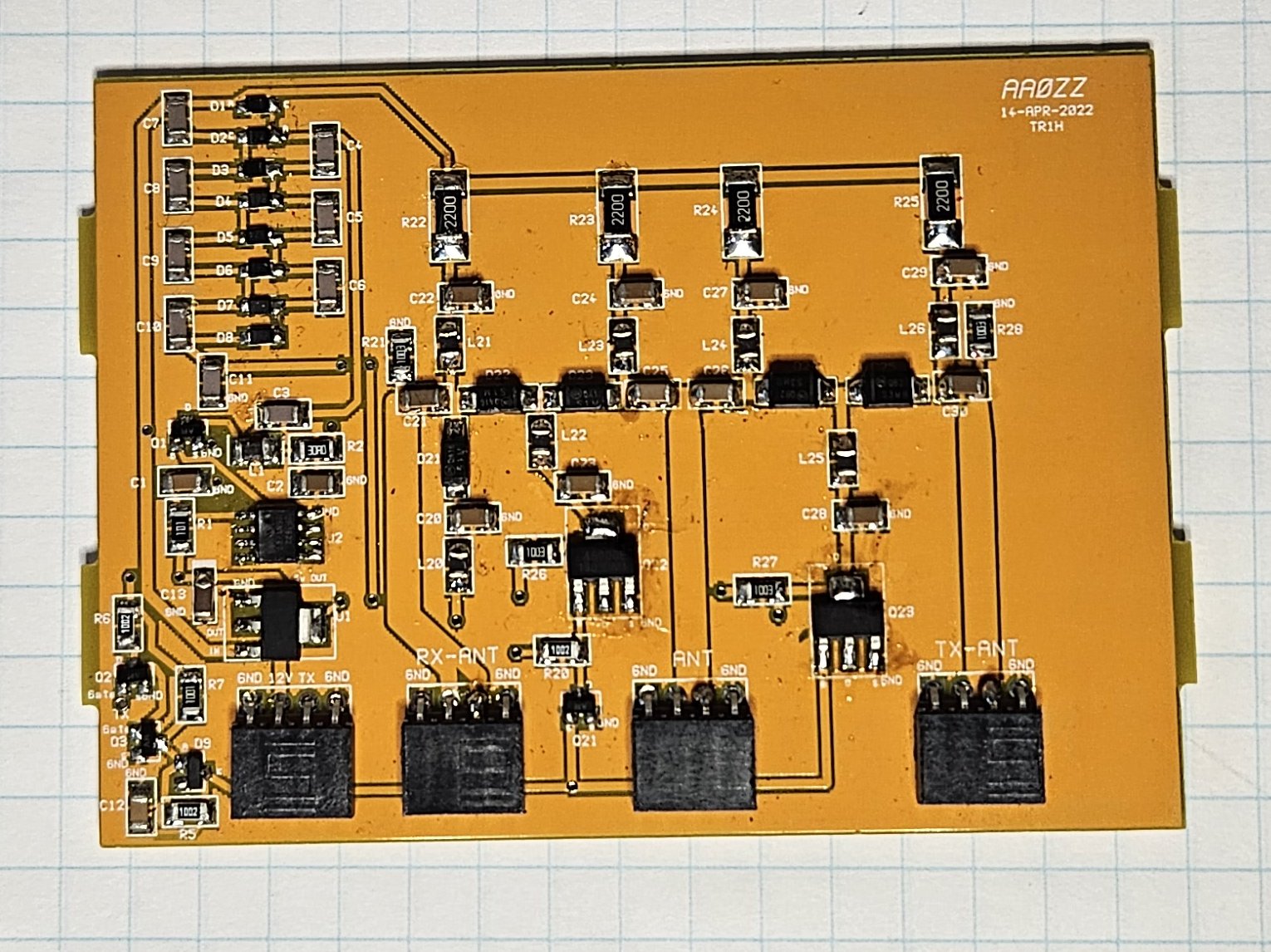
4b) High Power T/R Switch Schematic (JPG) This T/R switch is an overkill for a 30w transmitter but it's done in preparation for higher power. A simple PIC (12F1822) generates the 2 MHz
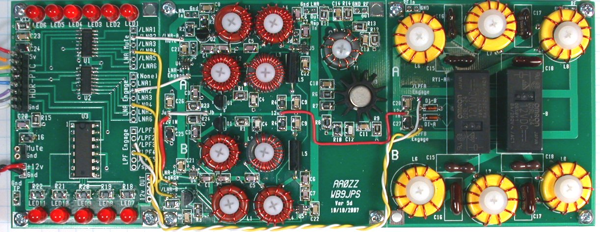
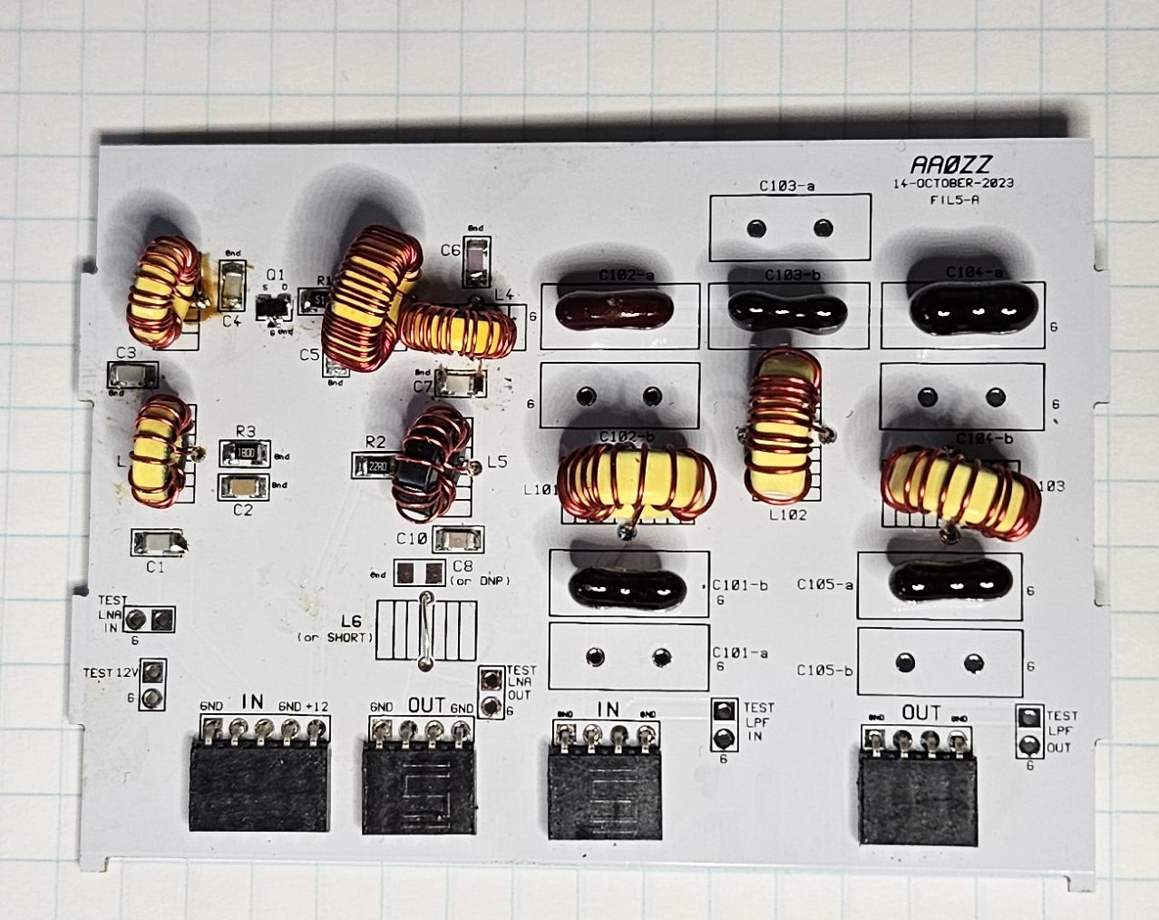
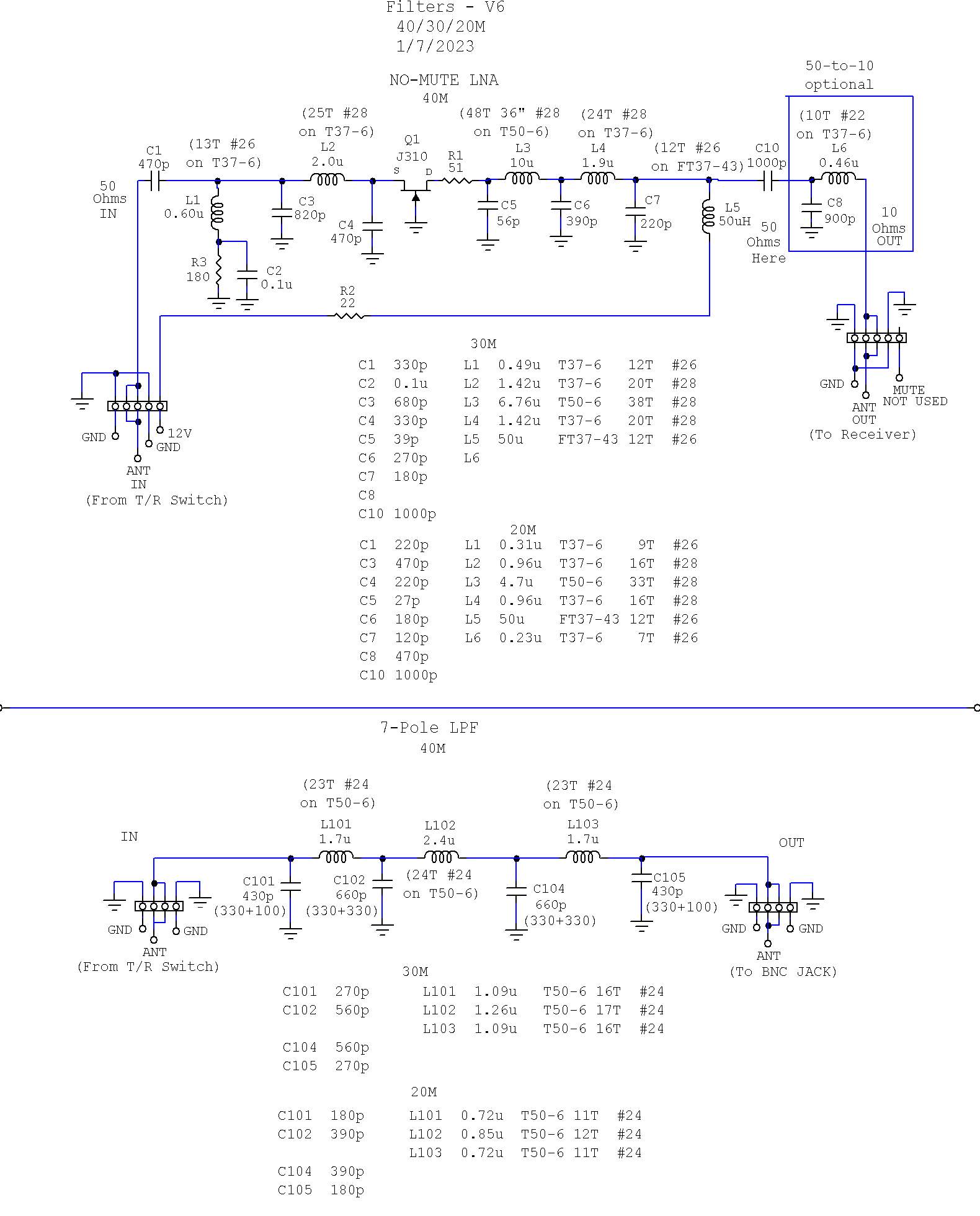
The T/R board has had 8 PCB revisions. 5b) Filter Board Schematic (JPG) The filter schematic shows component values for 40M, 30, and 20M. Low Noise Amplifier (LNA) circuitry is used on the RF input bandpass filters
in all three cases, even though the boost is probably not necessary for 40M. The LNAs were measured with a Spectrum Analyzer, showing that they provide about 10 dB of gain for the RF coming in.
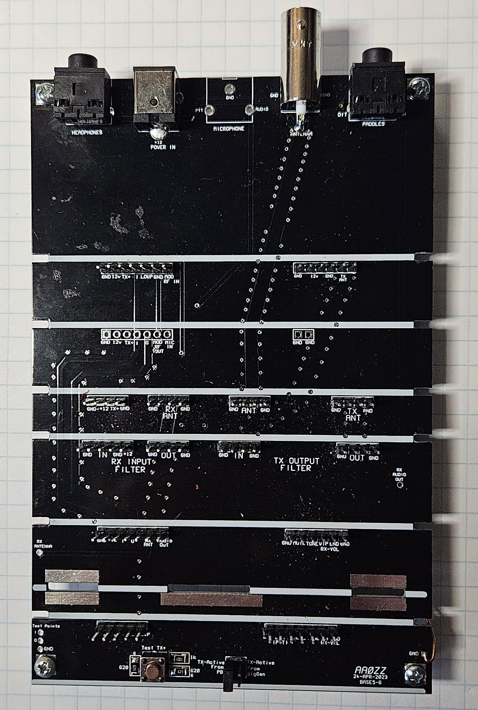
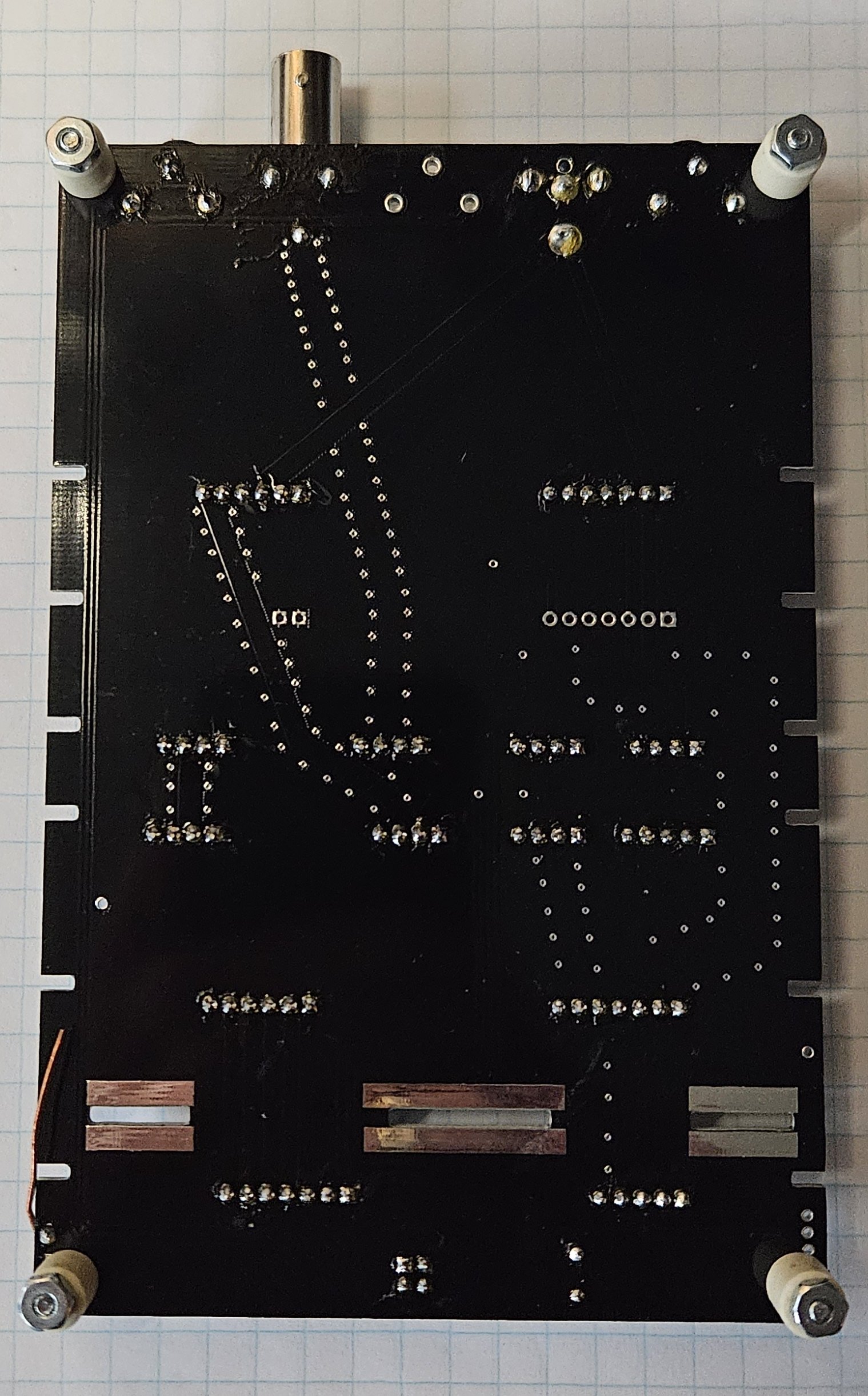
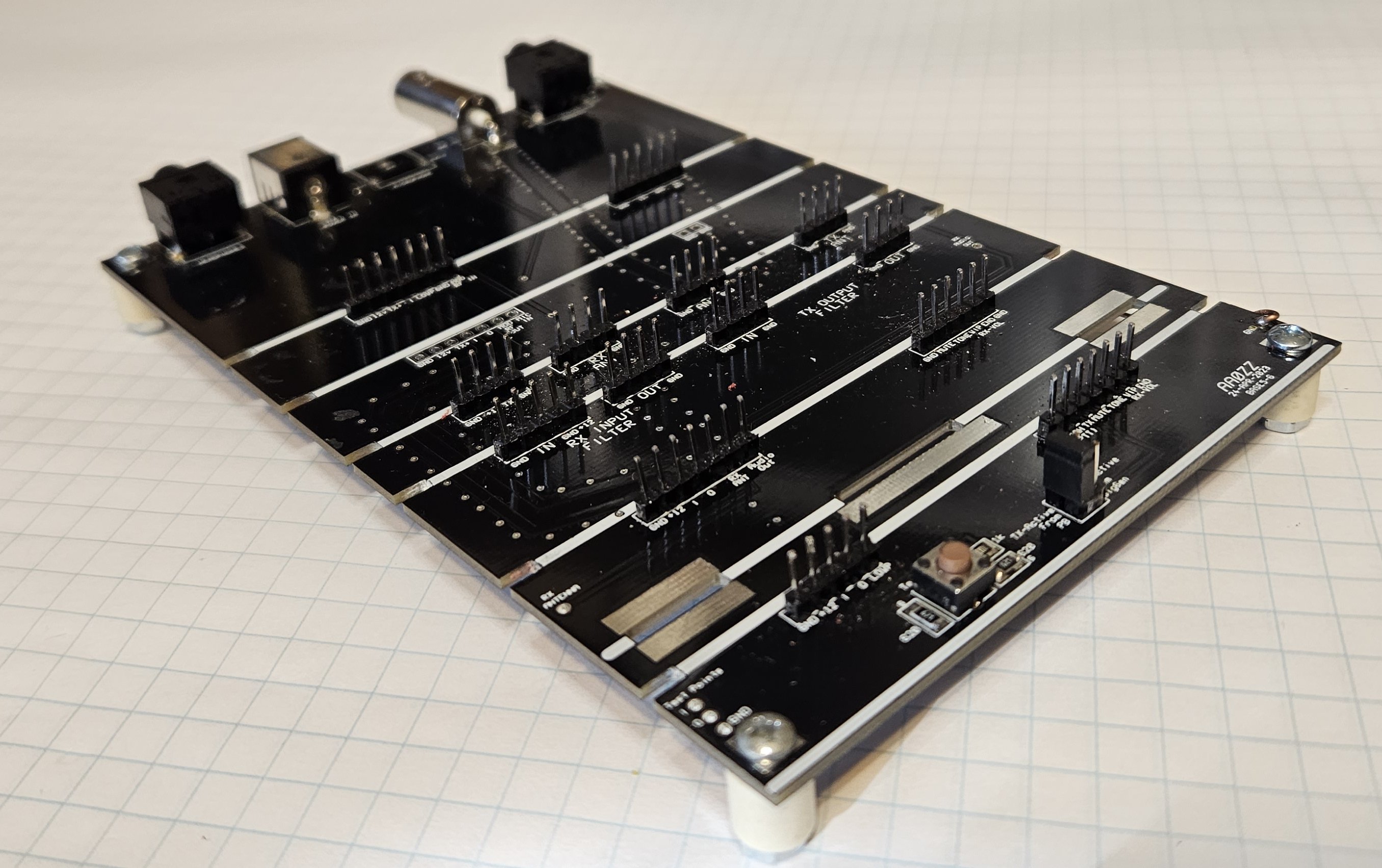
6a) Base board - top view (JPG) 6b) Base Board - bottom view (JPG) 6c) Base board diagonal showing Connectors (JPG) Note that there are NO "flying wires" between the boards; all board interconnections are in the base board.
The base board is double-sided copper with ground planes on both sides. Wide traces (approximately 50 ohms, with 110 mil width over 60 mil FR4 material)
are used for the RF traces. RF "stitching" was used along the long RF traces, although they probably aren't needed due to the frequencies
and the trace lengths relative to those frequencies. Some test components are installed on the base board for ease of testing.
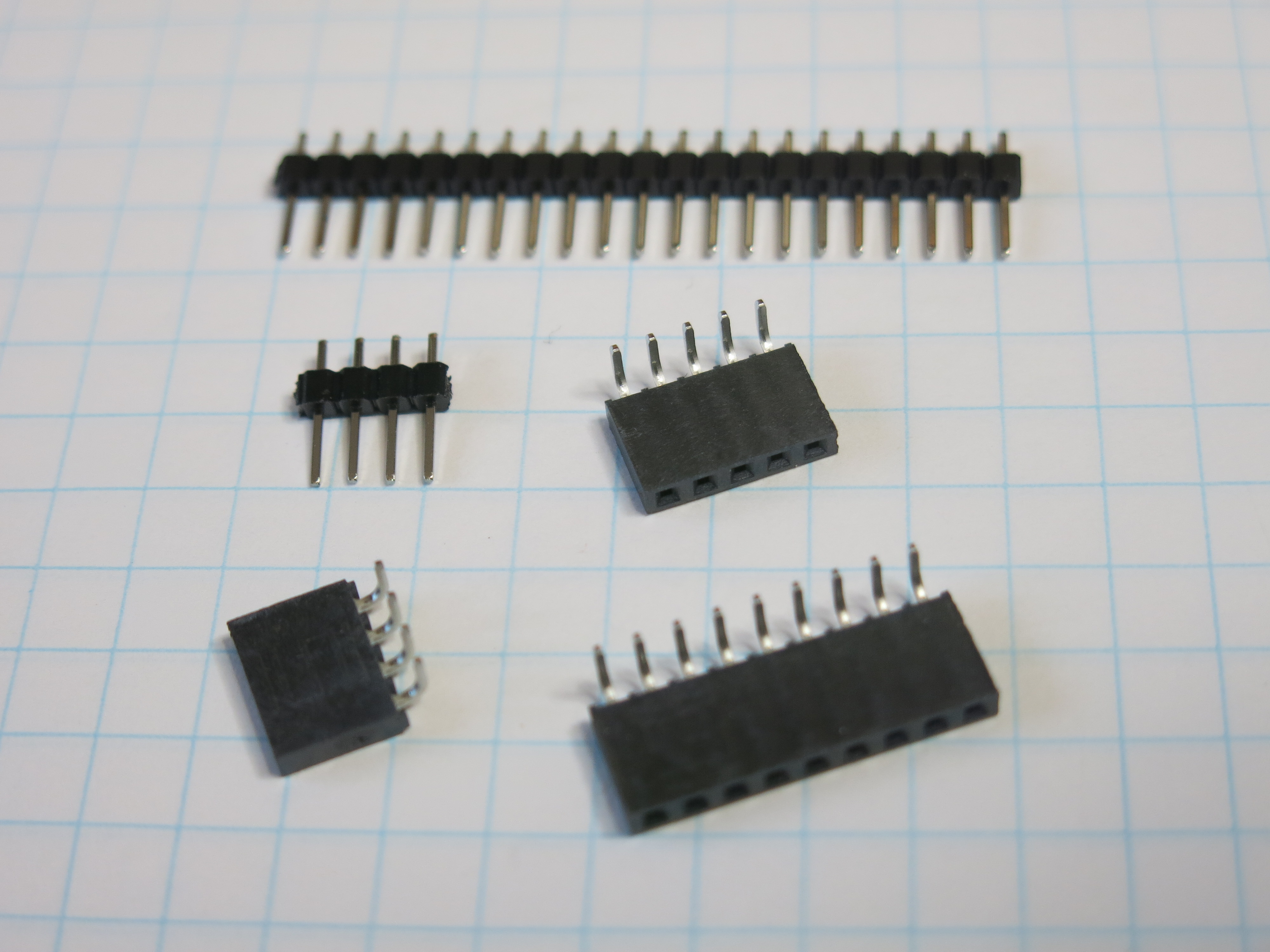
7) Board-to-board Connectors (JPG) NOTE: I wrote every line of code for the three PIC microcontrollers in assembler code. NO LIBRARIES!
As of 11/28/2023 I have "frozen" this version since it basically works on the air on 40M, 30M and 20M.
I've fed the speaker output into my computer and watched
the screenfull of waterfalls showing FT8 signals. I was able to decode FT8 as well as PSK31 signals.
That being said, I'm still battling some noise issues in the receiver during CW transmission. Might be a crosstalk issues.
I'm also working on a the SSB exciter plug-in board. It will use a slightly modified version of this transmitter with
the CW shaping circuitry disabled. A different band-specific plug-in filter board is used for each band.
Dimensions:
4" wide, 2.5" deep, 0.75" high (BLACK)
4.5" wide, 4" deep, 1.5" high (BLUE)
5.5" wide, 5" deep, 2" high (RED)
6.5" wide, 6" deep, 2" high (PURPLE)
Enclosure Assembly Manual (PDF)
(Click to enlarge)
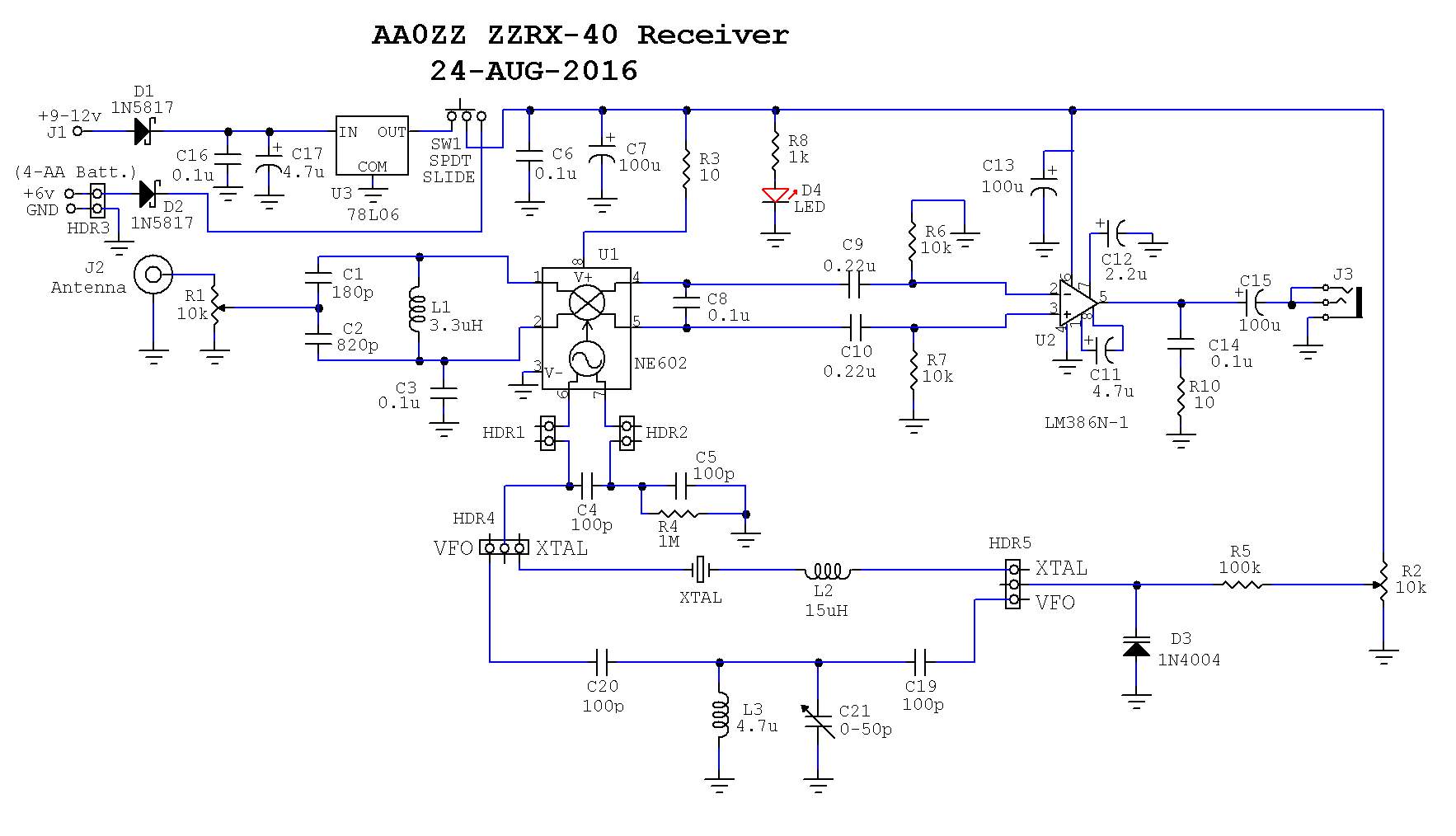
Schematic - ZZRX-40 Receiver (JPG format)
Theory Of Operation - Direct Conversion Receivers Including ZZRX-40 (PowerPoint .PPTX format)
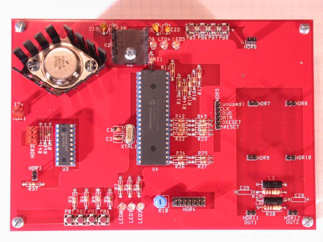
The AAØZZ EZKeyer III
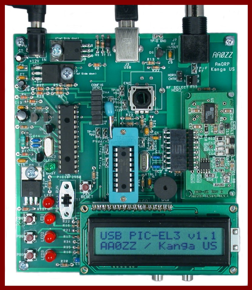
The PIC-EL III
Now with a USB Interface!
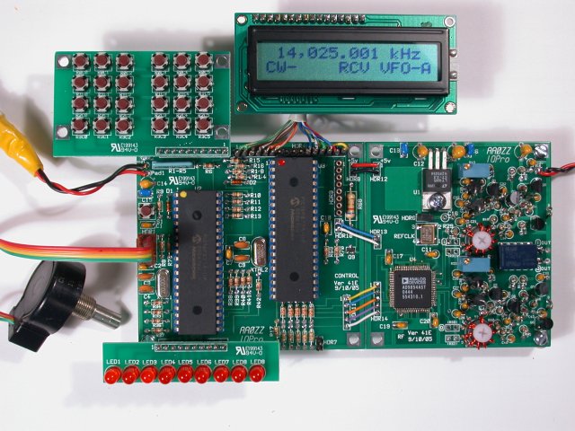
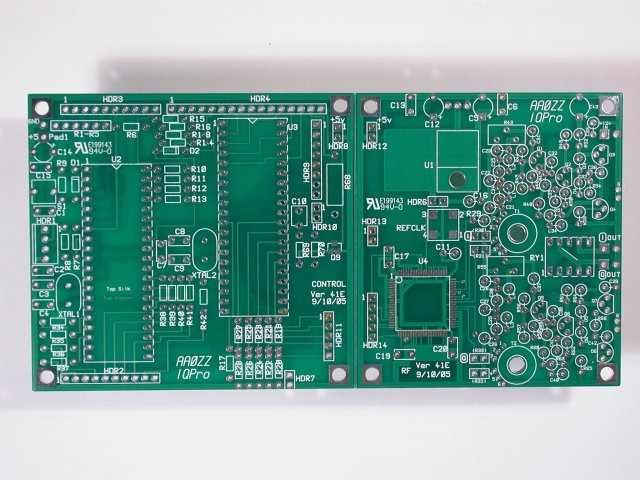
IQPro
LNA/LPF (for IQPro)
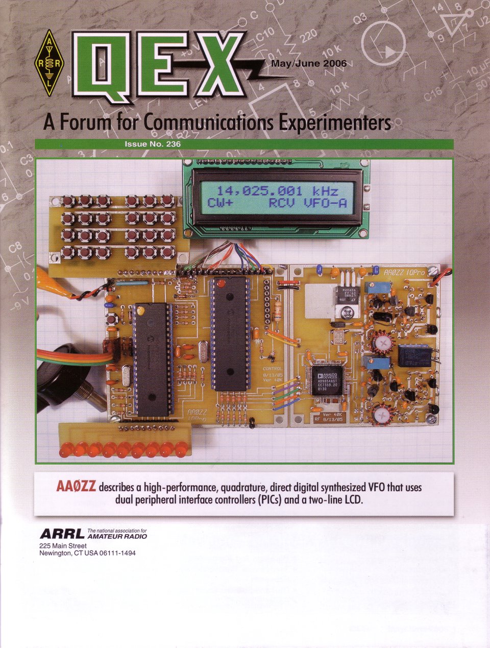
IQPro in May/June 2006 QEX magazine
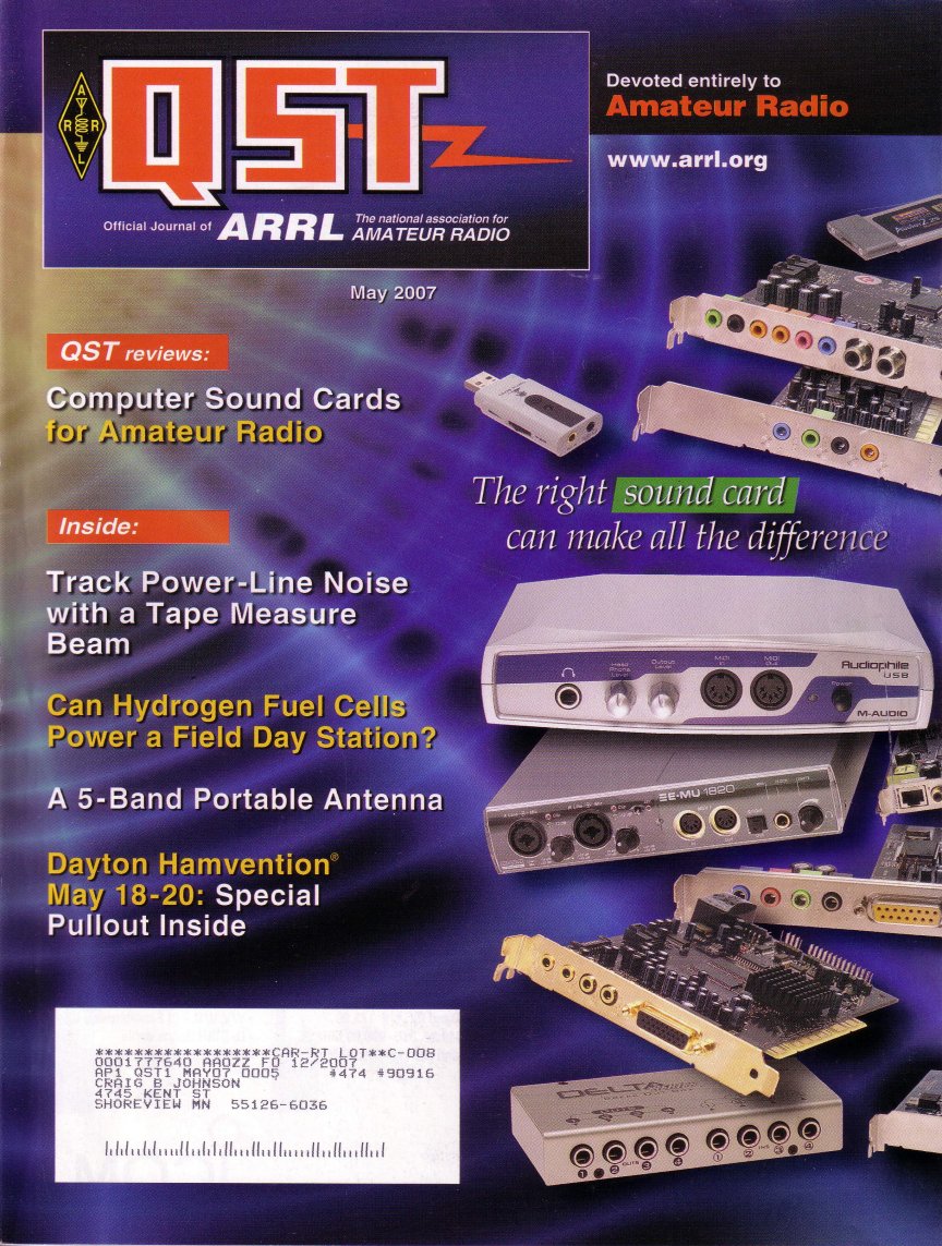
PIC-EL in May and June 2007 QST magazines
Part-1
Part-2
See my article about the IQPro in May/June 2006 QEX magazine above
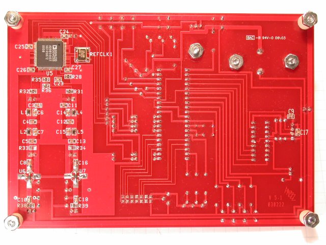
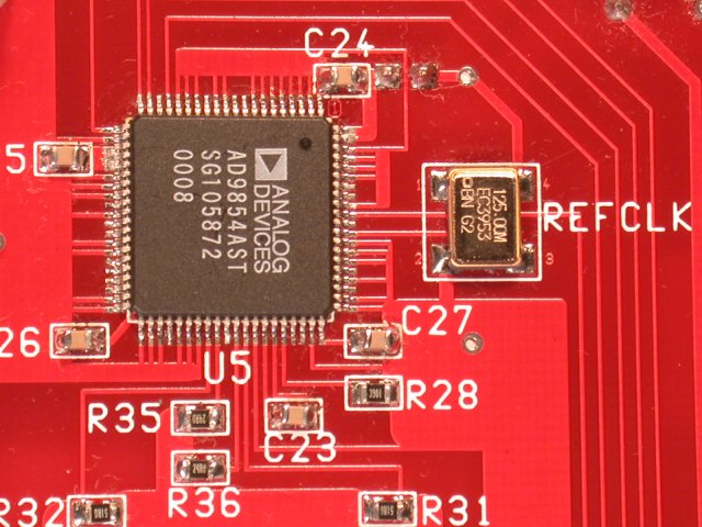
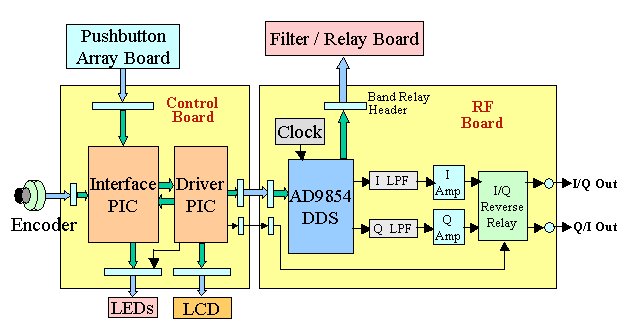
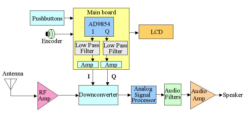
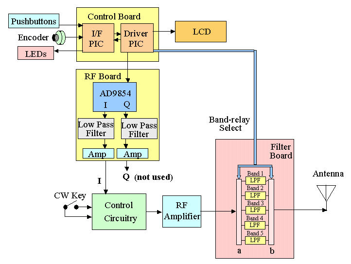
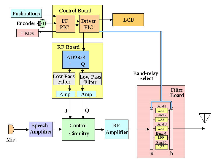
What is a DDS VFO? Very briefly, in simple terms, a Variable Frequency Oscillator (VFO) is an electronic 1) The IQPro is a 3" x 6" board, split into two halves. The "control" half
contains the two PICs and headers for the pushbuttons, LCD, LEDs, and band-switching. The "RF" half contains
the AD9854 DDS and the amplifiers. The intent is to allow the builder to put the RF portion into an "RF-tight"
box. This split also opens up the possibility of driving the "RF board" directly from a PC (serial or parallel
port) or from another control board.
2) The entire board runs on 5v (12v optional). Has a 3.3v regulator (no heat sink)
for the AD9854.
3) No MMIC amplifiers. Instead it has three options for boosting the AD9854's I
and Q outputs up to +7 dBm or higher. (Parts are supplied for all three options.)
Option 1: Toroids only. 12v power not needed. I and Q outputs of +7 dBm.
Option 2: Transistor amplifiers only. 12v power is needed. I and Q outputs
of +7 dBm.
Option 3: Toroids AND transistor amplifiers. 12v power is needed. I and Q
outputs of approximately +17 dBm.
4) No pushbuttons on the board (except a reset button). Instead it has a header
to support a 24 pushbutton array (4 rows x 6 columns) which is ready for easy customization and movement to the
front panel. The kit includes a PC board for mounting the pushbuttons but it is not required.
5) 12 pushbuttons (3 columns x 4 rows) form a telephone-like keypad for direct
frequency entry.
6) 12 additional pushbuttons for UP/DN MHz, UP/DN Band, VFO-A/VFO-B Toggle,
VFO-A = VFO-B, Fast-tuning toggle, Mode cycle (LSB, USB, CW-, CW+), Split toggle, Tone set, Backlight toggle,
and Calibrate toggle.
7) No LEDs on the board. Instead there is a header to support 9 LEDs to be
mounted on the front panel.
8) Nearly all through-hole parts. Exceptions are the AD9854, the 125-MHz
clock, and one MOSFET for enabling the LCD backlight.
9) Two 16F877 PICs, an Interface PIC and a Driver PIC. The Interface PIC
handles the encoder, the pushbuttons, the LEDs, and the band-switching. The Driver PIC handles the AD9854 and
the LCD. The two PICs "communicate" with messages.
10) Output signals are sent to a header when the VFO frequency changes to
a different frequency band. These signals can set/reset latching relays on an external board (not supplied) to
engage band-specific receiver pre-amps or transmitter output filters (for harmonic suppression).
11) A mode-cycle pushbutton operates a latching relay which reverses the I
and Q signals. If the mode is LSB or CW- the relay is latched in the "normal" position. If the mode is USB or CW+,
the relay is latched in the "reverse" direction.
12) Sidetone. The frequency is shifted (plus or minus) by a selected amount
when running in CW and Receive mode. The amount of offset (tone) is adjusted by pushing a pushbutton and then
turning the encoder. The tone value is saved in EEPROM so it is not lost by power-down. The offset value is
SUBTRACTED from the base (transmit) frequency if in CW- mode and ADDED to the base (transmit) frequency if in
CW+ mode. This allows you to listen to CW signals on either sideband.
13) LCD (16 x 2) with backlight toggled on/off via pushbutton.
14) 12v to 5v switching power supply kit included (about 1" square"). It is
meant to be mounted at some convenient location in the case.
15) The manual has MANY design details including the theory of operation,
reasons for design decisions, block diagrams, SPICE modeling of the amplifier, schematic, and a complete parts
list (almost all DigiKey part numbers).
16) FULL SOURCE CODE FOR THE TWO PICs IS SUPPLIED! This allows the builder
to completely understand how it works and to modify the operation to suit individual preferences.
Three options are being offered:
1) Full kit - $CALL
2) Bare board set (no parts - boards only) - $25 plus $2.50 s/h ($5 via Priority Mail)
2) Pre-programmed PICs (pair) - $25 plus $2.50 s/h ($5 via Priority Mail)
Please note that full kit includes the PC boards, printed manual, parts for the boards including
pre-programed PIC's, pre-mounted AD9854 chip, and a very high quality Clarostat optical (not mechanical)
encoder. Block Diagram of IQPro in Receiver
Block Diagram of IQPro in CW Transmitter
Block Diagram of IQPro in SSB Transmitter
IQPro Operations Manual (PDF format)
IQPro PIC microcode source code
Hint: Save the schematics on your hard drive and then open them with a picture viewer to see details.
WHAT IS IT? Multi-band LNA-LPF Explained
Multi-band LNA-LPF Board Picture
Multi-band LNA-LPF Parts List (Excel Format)
IQPro Phase Noise
Measurements (Rev-1 8/5/2006) - by Gary Johnson, WB9JPS
Wes Hayward, W7ZOI, comments
regarding WB9JPS analysis of IQPro
WB9JPS - Gary Johnson (8/7/2006)
W6JL - Don Huff (updated 8/16/2008)
K5EMI - Bill Stewart (5/27/2007)
KA8RIZ - Steve Geary (3/25/2007)
AB7O - Wayne Thurston (6/12/2007)
AA3SJ - Ed Kessler (link to Ed's page 3/24/2007)
WB9JPS - Gary Johnson (link to Gary's page 11/12/2007)
K8AC - Floyd Sense (link to Floyd's page 1/3/2008)
Join us there and ask questions! Or E-mail me. (Address below.)
IQPRO
(Click to enlarge)
Designed by Craig, AAØZZ and Bruce, AAØED See my YAHOO Group: DDS-VFO for Support / Discussion / Files / Pictures / Documentation
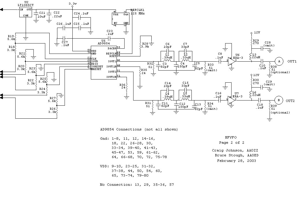
Complete Manual: Manual Ver 1.0f (in PDF format) Updated 01/31/05
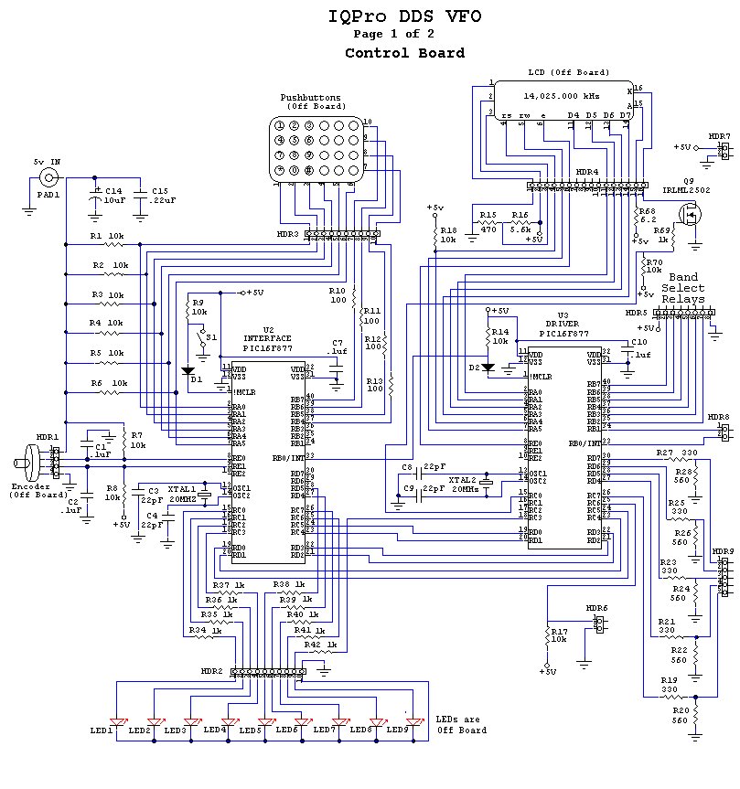
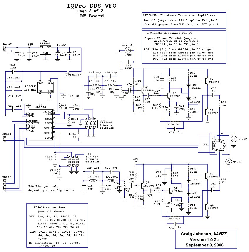
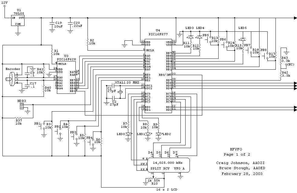
Schematic: Page 1 of 2 (drawn with CircuitMaker)
PIC16F877 Symbolics v5.19b
HEX (Main Control)
PIC16F628 Symbolics v1.1c
HEX (Encoder)
Parts List (updated 11/13/2004 - with prices)
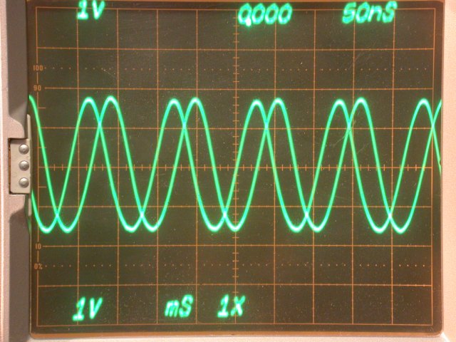
Perfect quadrature output! (0 - 30 MHz)
Performance Analysis (PDF) New 01/31/05
Don Huff, W6JL, uses a HFVFO prototype with R2Pro
PowerPoint slides from my FDIM Presentation on May 15, 2003
Sorry, but the IQ-VFO kits are sold out and no longer available from AmQRP.
HFVFO board - top
HFVFO board - bottom
HFVFO board - AD9854
HFVFO board - running
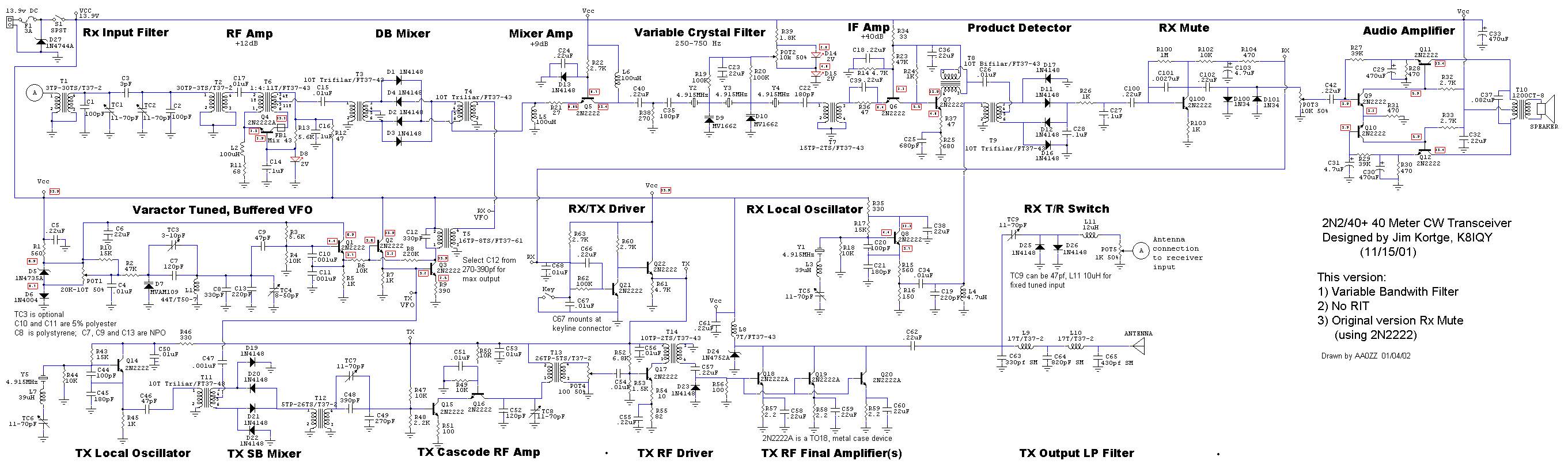
Design details at Jim Kortge's home page: K8IQY's 2N2 Homepage
Schematic (drawn with CircuitMaker)
My 2N2-40 Layout (PowerPoint format - to download and print - actual size)
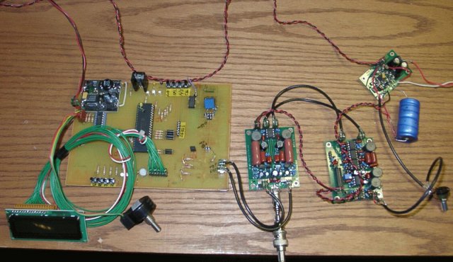
My 2n2-40 transceiver
(Click to enlarge)
Yes, it works!
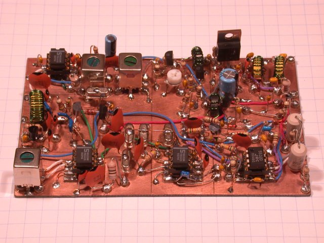
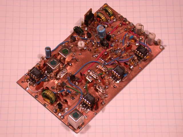
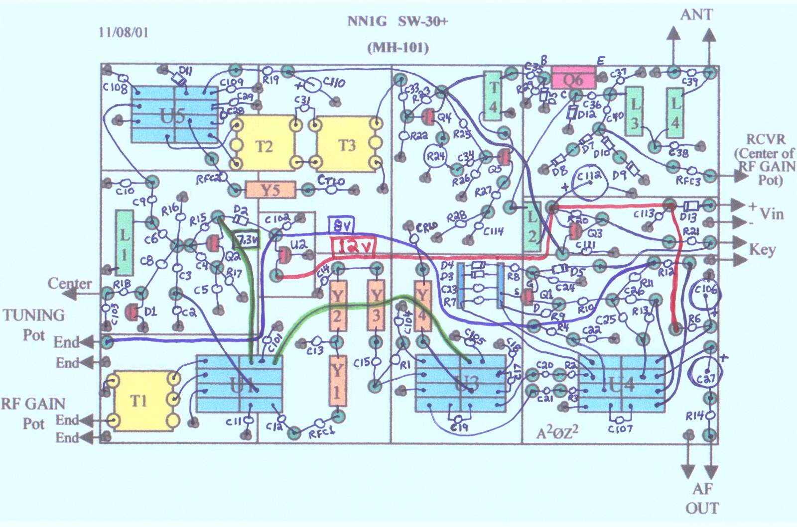
My MH101 ("manhattan" style) version of the SW 30+ Picture 1 Picture 2
- Pad layout in PowerPoint format (actual size): MH101 Pad Layout
- All parts layout: All Parts
My MH101 transceiver
(Click to enlarge)
Yes, it works too!
Great are the works of the Lord;
they are pondered by all who delight in them.
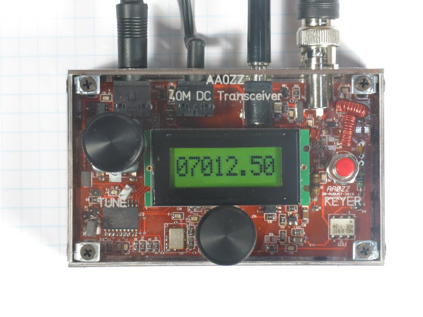
shortly after I developed an "Altoids-size" enclosure for the 4SQRP Group to sell as a fund-raiser for OzarkCon.
This box is 4" x 2.5" x 0.75"
be loosely patterned after the Roy Lewallen's (W7EL) famous 40M Optimized Transceiver but should have a
digital front-end to generate the RF instead of his analog oscillator and then use a rotary encoder to change the
frequency. With a digital front-end it's easy to add an LCD to display the frequency.
He also used the Arduino to control his rotary encoder, LCD and his keyer. He was on the air very quickly.
oscillator. The same PIC was used for a rotary encoder to change frequency and a small, 1x8 character LCD.
to generate the CW DITs and DAHs.
components are surface mount (SMT), size 0805.
simple Direct Conversion receivers do not have opposite-side suppression they take a little extra care when making
contacts.
Fast QSK is very important to me so I paid a lot attention to this when designing the main PIC code. I check often in the code's "main path" to detect as quickly as
possible a switch from transmit to receive or back to transmit. I change frequencies on the switch of course, to give a 600 Hz offset during receive so as to be able to hear
the other station's signals when the two transmitters are on the same frequency (i.e, zero beat) as they should be. This means there is a "lot of work to do" when switching
between transmit and receive modes and this rig can still do it all in 8 ms.
pulses for the charge pump which develops 150 v (loaded) for back-biasing the PIN diodes. This T/R switch can easily handle 100w.
![]()

ZZRX-40 PCB
ZZRX-40 PCB in Case
ZZRX-40 Complete
PIC Microcontroller Programmer and Development Board
(More info below.)

mechanism that creates a sine wave at a desired frequency. This VFO is designed to be used as
a "tuner" for a radio transmitter or receiver. VFOs are often constructed using variable
capacitors or coils that are moved to change the frequency but this VFO uses a newer technology, a
very tiny Direct Digital Synthesis (DDS) chip, controlled by a small computer (microcontroller),
to create the sine wave at the desired frequency.
Contact me. I still have all of the "key components" available. See details at the top of this web page.
Multi-band LNA/LPF Board for IQPro (NEW!)
IQPro Performance Reports / Measurements
IQ-VFO and IQPro User Pages
 2N2-40 (40 Meter transceiver - designed by Jim Kortge, K8IQY)
SW-30+ (30 Meter transceiver - designed by Dave Benson, K1SWL)

.jpg)
.jpg)
Biographical sketch (updated 5/2022): AAØZZ Bio
Send me E-Mail at:
Go to my personal, non-ham home page at
www.cbjohn.com
Last Updated 22-December-2023
Hit count since 6/2021
I created this web page entirely with a text editor!
![]()
(Sorry I had to show the Email address like this. I'm sure you know why.)
- Craig, AAØZZ
Why? It's just because of my curiosity about how HTML works!